Silicon Germanium Epitaxy
News
| 3 Jun | 2021 | A singlet triplet hole spin qubit in planar Ge The IST Austria, in collaboration with the SiGe group and researchers from Barcelona and Konstanz, demonstrates a hole spin qubit in a double quantum dot device. With two spin-1/2 particles, the singlet |S⟩ = (|↑↓⟩-|↓↑⟩)/√2 and the unpolarised triplet |T0⟩ = (|↑↓⟩+|↓↑⟩)/√2 form the two computational-basis qubit states |0⟩ and |1⟩. In a weak magnetic field, electrically-tunable energy splitting between the ↑ and ↓ spin states in the two quantum dots allows the total spin state of the double quantum dot to be manipulated with nanosecond radiofrequency pulses. These short pulses means the qubit operations are very fast, while the long lifetime (150 μs) means that there would be time to perform complicated quantum computations. The state of the qubit can then be read electrically since the |S⟩ state allows current to tunnel through, while current is blocked by the |T0⟩ state. The use of an especially weak magnetic field - other work uses fields which are at least ten times stronger - would allow integration of these qubits with superconductors. The research is published in Nature Materials. DOI: 10.1038/s41563-021-01022-2. 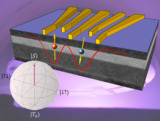 |
| Sep | 2014 | Posters presented at MNE 2014 and XTOP 2014. |
| 23 June | 2014 | The generation of two
complementary spin-up and spin-down electron
populations can be obtained by illuminating a semiconductor through a
patterned metal mask as shown in the Nature Materials
paper by an L-NESS-Physics Department and CNR
team
|
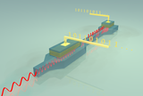
| 12 May | 2014 | The fabrication of germanium-based modulators, detectors and waveguides on a silicon wafer offers an attractive platform for on-chip interconnects: the Silicon Photonics group of the University Paris Sud, in collaboration with the SiGe group, publishes in Nature Photonics.
La Repubblica (Italian) La Provincia: Como, supermicrochip: Il Politecnico batte Stanford (in Italian) |
| 13 May | 2013 | The SiGe group is featured on TG Leonardo. |
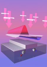
| 15 Apr | 2013 | Germanium is the laser material of the future
Researchers at the Politecnico together with the ETH Zurich and the Paul Scherrer Institute (Switzerland) have demonstrated how germanium can be transformed into a laser material. By making micro-bridges of germanium in which the reduction of the cross-section of the bridge at a constriction concentrates the pre-existing thermal stress left behind by the growth process, the bandgap is modified in a way which turns germanium into an efficient light emitter. The research is published in Nature Photonics 
Tom's Hardware (Italian) Lombardia News (Italian) Corriere della Sera (Italian) ANSA (Italian) Photonics.com Scicasts.com Science Daily |
| 10 Sep | 2012 | Built-in germanium lasers could make computer chips faster - research published in Physical Review Letters in collaboration with the PSI and ETH Zürich in Switzerland, highlights the conditions under which a germanium laser could be realized. |
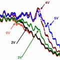
| 8 Jun | 2012 | High-speed germanium quantum well modulator - Using high germanium content compounds is a promising approach to obtain efficient, high-speed modulation.
 |
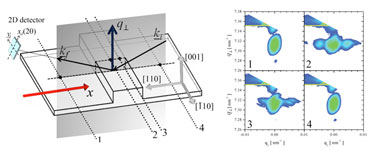
| 4 May | 2012 | X-ray diffraction maps uniaxial strain in a single nanostructure, work performed at ESRF beamline ID13 as a collaboration between the Nanoscale Device and SiGe epitaxy groups
 |
| 16 Mar | 2012 | The SiGe epitaxy group makes the cover of Science for its work on Scaling Hetero-Epitaxy from Layers to Three-Dimensional Crystals in collaboration with the ETH Zürich, the Università di Milano-Bicocca and the Centre Suisse d'Electronique et de Microtecnique at Neuchâtel
In arrivo nuovi materiali: semplicemente “perfetti” Ricercatori italiani sulla copertina di Science: con la loro tecnica più facile produrre materiali per l'hi-tech Il futuro della tecnologia su nano-colonne di Como Il materiale perfetto? Nasce a Milano ed è figlio della fortuna Submicrometre diffraction in dense arrays of three-dimensional germanium crystals: an ESRF Spotlight on Science Communicato stampa: Materiali perfetti? Ecco come ottenerli 
The cover of the 16th March issue of Science, featuring Ge crystals grown by LEPECVD on Si pillars. The growth was carried out at the L-NESS by Claudiu Falub, visiting from the ETH Zürich, and this scanning-electron microscopy image was taken by Claudiu at the ETHZ FIRST laboratory. |
| 1 Aug | 2010 | The GREEN Silicon FET-Proactive EU Project begins, with the SiGe epitaxy group playing a fundamental role |
| 1 Nov | 2009 | The 8th ESPS-NIS will be held in Como, 14-18th June 2010 |
| 7 Apr | 2008 | Il Sole 24 ORE visit the L-NESS |
People
- Giovanni Isella, group leader
- Daniel Chrastina, associate professor
- Jacopo Frigerio, researcher
- Andrea Ballabio, Post-doc
- Hans von Känel, consultant
Former group members
- Valeria Mondiali, PhD student
- Stefano Cecchi, post-doc
- Fabio Isa, PhD student, now a post-doc at the ETH Zürich
- Claudiu Falub, visiting researcher
- Tamara Moiseev, researcher
- Marcello Ferretto, Master's student
- Marco Fiocco, Masters student, now a PhD student in the Nanoscale Device Group
- Carlo Pozzi, Masters student
- Valeria Montuori, Masters student
- Lario Martinelli, technician
Research
- SiGe multilayers for thermoelectric applications
- SiGe islands on pit-patterned substrates
- Ge layers on pre-patterned substrates
- Multiple quantum wells for optical applications
- Doped and intrinsic Ge layers
- High mobility Ge quantum wells
- Virtual substrates
- Nanocrystalline Si for photovoltaic applications
SiGe multilayers for thermoelectric applications
The primary objective of the GREENSi project is to demonstrate integrated on-chip thermoelectric energy harvesting using micro-/nano-fabricated Si/SiGe nanostructures with improved efficiencies through the use of bandstructure engineering and phonon bandgaps. High performance thermoelectric materials require high electrical conductivity and low thermal conductivity. Our approach is to engineer thermoelectric materials which enhance the electrical conductivity while simultaneously blocking the tranport of thermal energy through the devices. Bulk 2D Si/SiGe superlattices, laterally patterned 1D nanowires and 0D quantum dots made from Si/SiGe heterostructure technology will be investigated for high performance thermoelectrics in microsystems and other applications. We propose to combine the optimum 2D superlattice or 0D quantum dot material with 1D nanowire patterning to further improve the thermoelectric performance of microgenerators. The final optimised thermoelectric generator will be integrated with a capacitor energy store on a mm-sized single silicon chip to demonstrate a power source for an autonomous system. This will be used to power a micropower CMOS sensor to demonstrate its use as an energy harvesting system. The developed technology will be compatible with the power supply requirements for wireless autonomous systems such as those defined in the IEEE 802.15.4 standard. While the project is aimed at on-chip sustainable energy generation, the techniques, technology and IP being developed will also be able to be deployed into high efficiency (>20%) thermoelectric generators and Peltier coolers for domestic and industrial applications.

A schematic diagram showing a thermoelectric generator and the insert shows a magnified image of a single thermoelectric module using nanofabricated structures.
SiGe islands on pit-patterned substrates
Silicon substrates patterned by the Nanoscale Device Group using electron-beam lithography and reactive-ion etching are used as templates for the growth of Ge dots by low-energy plasma-enhanced chemical vapour deposition (LEPECVD).
Ge layers on pre-patterned substrates
The SiGe epitaxy group has been featured on the cover of Science for its work on the growth of Ge crystals on pre-patterned Si pillars, in collaboration with the ETH Zürich, the Università di Milano-Bicocca and the Centre Suisse d'Electronique et de Microtecnique at Neuchâtel.

The cover of the 16th March issue of Science, featuring Ge crystals grown by LEPECVD on Si pillars. The growth was carried out at the L-NESS by Claudiu Falub, visiting from the ETH Zürich, and this scanning-electron microscopy image was taken by Claudiu at the ETHZ FIRST laboratory.
Multiple quantum wells for optical applications
Current ICT is dominated by silicon because of its physically and electronically advantageous properties as well as its nearly unlimited availability. However, today's demand for ever-increasing data rates requires switching speeds beyond those which state-of-the-art electronics provide. Electronic Photonic integrated circuits (EPICs) on Si are probably the most promising answer to this challenge. A CMOS-compatible laser based on a group IV material is therefore extremely desirable if not mandatory to complete the monolithic integration of electronics and photonics. Only a few years ago this idea was generally considered an engineer's dream and many scientists even discarded the idea as completely impractical. However, several very recent observations have accelerated the research in this field. In particular, the fully CMOS-compatible (group III-V free) optically pumped Ge-on-Si laser demonstrated at the MIT is a mayor step towards finally realizing a complete optoelectronic platform on Si. CMOS-compatible monolithically grown lasers are the “missing link” needed for the realization of an EPIC going beyond state-of-the-art as Si-based detectors, waveguides, and modulators are well established. Completing this technology will enable extended multi-core parallel computing with integrated lasers used for data distribution between individual cores. Another practical advantage of the Ge material system in connection with innovative thermally induced strain and n-type doping is its emission in the 1.55 μm C-band of fibre optic communications, ensuring compatibility with existing telecommunication infrastructure.
SiGe multiple quantum well (MQW) heterostructures grown by LEPECVD have demonstrated direct-gap photoluminescence at low temperature and at room temperature and above, electroluminescence at room temperature, the quantum-confined Stark effect, and transient gain.
Doped and intrinsic Ge layers
High mobility p-type modulation doped quantum wells
A low-temperature mobility of 120 000 cm2V-1s-1 has been measured in a strained Ge channel grown by LEPECVD, at a sheet density of 8.5×10⁻¹¹ cm-2, beating both the previous LEPECVD record and the best material obtained by molecular-beam epitaxy.

Low-temperature mobilities of strained Ge layers grown by LEPECVD. The lines represent calculations of the scattering rate based mainly on ionized dopants, with a variation in the background doping.
These mobilities are made possible in part by the high epitaxial growth rates available to LEPECVD, and also by the high quality of the virtual substrate.
Virtual substrates
Relaxed graded silicon germanium buffer layers greatly extend the possibilities of the silicon germanium material system. Such a relaxed buffer layer, or virtual substrate, allows the growth of a tensile strained silicon quantum well for n-type conduction. Also, it is possible to grow compressively strained quantum wells for p-type conduction with any germanium fraction.
The traditional method of producing a virtual substrate is to linearly increase the germanium fraction x at around 10% per micron (E. A. Fitzgerald et al. Appl. Phys. Lett. 59 [7] 811-813 [1991]). LEPECVD is excellent for this purpose, since growth rates of 5-10 nms-1 can be reached. This means that a buffer which is graded at 7% per micron from pure Si to pure Ge, and capped with 2 microns of pure Ge, still takes less than one hour to grow. The threading dislocation density of such a buffer has been measured to be 1.5×105 cm-2 and the rms surface roughness is 3.2 nm (S. G. Thomas et al. J. Electron. Mater. 32 [9] 976-980 [2003]). For comparison, the threading dislocation density of a similar buffer grown by ultra-high vacuum chemical vapour deposition (UHV-CVD) is 2.1× 106 cm-2 (and the rms roughness is 24 nm) but here the wafer has to be taken out of the growth system half-way through and subjected to chemical-mechanical polishing (CMP) (S. B. Samavedam et al. Appl. Phys. Lett. 73 [15] 2125-2127 [1998]).
Such structures can have excellent electrical properties (B. Rößner et al. Appl. Phys. Lett. 82 [5] 754-756 [2003], B. Rössner et al. Appl. Phys. Lett. 84 [16] 3058-3060 [2004]). These papers feature modulation-doped strained Ge channels on 70 % virtual substrates.
Nanocrystalline Si for photovoltaic applications
Facilities
LEPECVD
Low-energy plasma-enhanced chemical vapour deposition (LEPECVD) is a technique for growing high-quality epitaxial or nanocrystalline SiGe layers at high rates, with efficient use of the source materials.

Schematic of the LEPECVD system.

The original prototype LEPECVD system.
The original LEPECVD prototype was brought to the L-NESS in Como from the ETH Zürich in 2002. It can handle wafer sizes up to 4” (100 mm), and smaller sizes by means of suitable Mo adaptor plates.
LG2: Second generation LEPECVD

The second generation LEPECVD system (LG2).
This system was developed, built and optimized at the L-NESS. It can take wafer sizes up to 8” (200 mm).
X-ray diffraction
The group is equipped with a high-resolution x-ray diffractometer, which is used to measure the lattice constants of epitaxial SiGe layers and to thereby characterize their composition, strain and thickness.
Atomic force microscopy
The group is equipped with a Veeco Innova atomic force microscope. The microscope is used to characterize the surface morphology of as-grown SiGe layers, and to image etch pits following defect etching.
He cryostat
The group is equipped with a Cryogenic cryogen free (i.e., a closed cycle liquid helium-4) magnet system to 7.5 T with an integrated variable temperature insert. The lowest temperature which can be reached by this cryostat is about 1.4 K. The cryostat is connected to a transport measurement system comprised of digital source meters, multi meters, preamplifiers, function generators, an oscilloscope, and an acquisition board. This system is used for the characterization of high-mobility heterostructures.
Publications
- D. Marris-Morini, G. Z. Mashanovich, M. Nedeljkovic, C. Alonso-Ramos, L. Vivien, J. Frigerio, and G. Isella: Germanium-based mid-infrared integrated photonics, Laser Photon. Rev. 2026, e01738 (2026).
- A. Bricout, M. Bertrand, P. Täschler, B. Schneider, V. Turpaud, S. Calcaterra, D. Impelluso, M. Faverzani, D. Bouville, J.-R. Coudevylle, S. Edmond, E. Herth, C. Alonso-Ramos, L. Vivien, J. Frigerio, G. Isella, J. Faist, and D. Marris-Morini: Pulse generation by on-chip dispersion compensation at 8 μm wavelength, Laser Photon. Rev. 2025, e01485 (2025).
- M. Botifoll, I. Pinto-Huguet, E. Rotunno, T. Galvani, C. Coll, P. H. Kavkani, M. C. Spadaro, Y.-M. Niquet, M. B. Eriksen, S. Martì-Sànchez, G. Katsaros, G. Scappucci, P. Krogstrup, G. Isella, A. Cabot, G. Merino, P. Ordejón, S. Roche, V. Grillo, and J. Arbiol: Artificial intelligence-assisted workflow for transmission electron microscopy: From data analysis automation to materials knowledge unveiling, Adv. Mater. 2025, e06785 (2025).
- M. Faverzani, D. Impelluso, S. Calcaterra, C. Zucchetti, D. Chrastina, C. Tassi, G. Capellini, P. Biagioni, G. Isella, M. Virgilio, and J. Frigerio: Mid-infrared intersubband transitions in p-type SiGe parabolic quantum wells.Adv. Opt. Mater. 2050, e03060 (2025).
- B. van Straaten, F. Fedele, F. Vigneau, J. Hickie, D. Jirovec, A. Ballabio, D. Chrastina, G. Isella, G. Katsaros, and N. Ares: All-rf-based coarse-tuning algorithm for quantum devices using machine learning, Phys. Rev. App. 24, 054030 (2025).
- V. Wadhia, F. Meier, F. Fedele, R. Silva, N. Nurgalieva, D. L. Craig, D. Jirovec, J. Saez-Mollejo, A. Ballabio, D. Chrastina, G. Isella, M. Huber, M. T. Mitchison, P. Erker, and N. Ares: Entropic costs of extracting classical ticks from a quantum clock, Phys. Rev. Lett. 135, 200407 (2025).
- M. Silvestre, S. Lacaze, A. Gilbert, S. Calcaterra, A. De Cerdeira Oliveira, D. Impelluso, G. Isella, J.-B. Rodriguez, and E. Tournié: MBE growth of GaSb on Ge-based templates grown on Si for mid-infrared photonics [invited], Opt. Mater. Express 15, 2499 (2025).
- S. Freddi, N. Granchi, M. Gherardi, R. Giani, G. Calusi, C. Gonzini, L. Forcieri, A. Fedorov, G. Isella, F. Intonti, M. A. Vincenti, and M. Bollani: Assisted dewetting of pure Ge nanostructures for Mie-resonant all-dielectric photonics, Opt. Express 33, 37509 (2025).
- K. Aggarwal, A. Rolandi, Y. Yang, J. Hickie, D. Jirovec, A. Ballabio, D. Chrastina, G. Isella, M. T. Mitchison, M. Perarnau-Llobet, and N. Ares: Rapid optimal work extraction from a quantum-dot information engine, Phys. Rev. Research 7, L032017 (2025).
- S. Calcaterra, M. Faverzani, D. Impelluso, D. Chrastina, R. Giani, L. Anzi, J.-H. Bae, C. Tassi, D. Buca, P. Biagioni, G. Isella, M. Virgilio, and J. Frigerio: Optical and structural properties of p-doped Ge/SiGe multiple quantum wells for mid-infrared photonics.Phys. Rev. B 112, 045429 (2025).
- J. Saez-Mollejo, D. Jirovec, Y. Schell, J. Kukucka, S. Calcaterra, D. Chrastina, G. Isella, M. Rimbach-Russ, S. Bosco, and G. Katsaros: Exchange anisotropies in microwave-driven singlet-triplet qubits, Nature Communications 16, 3862 (2025).
- S. Freddi, M. Gherardi, A. Chiappini, A. Arette-Hourquet, I. Berbezier, A. Fedorov, D. Chrastina, and M. Bollani: Strain-driven dewetting and interdiffusion in SiGe thin films on SOI for CMOS-compatible nanostructures, Nanomaterials 15, 965 (2025).
- M. Janík, K. Roux, C. Borja-Espinosa, O. Sagi, A. Beghdadi, T. Adletzberger, S. Calcaterra, M. Botifoll, A. Garzón Manjón, J. Arbiol, D. Chrastina, G. Isella, I. M. Pop, and G. Katsaros: Strong charge-photon coupling in planar germanium enabled by granular aluminium superinductors, Nature Communications 16, 2103 (2025).
- J. Pedrini, M. Cis, E. Talamas Simola, E. Bonera, G. Isella, and F. Pezzoli: Ge-based photonics for quantum technologies.In 2024 IEEE Photonics Society Summer Topicals Meeting Series (SUM), 1--2 (2024).
- F. De Palma, F. Oppliger, W. Jang, S. Bosco, M. Janík, S. Calcaterra, G. Katsaros, G. Isella, D. Loss, and P. Scarlino: Strong hole-photon coupling in planar Ge for probing charge degree and strongly correlated states, Nature Communications 15, 10177 (2024).
- J. Hickie, B. van Straaten, F. Fedele, D. Jirovec, A. Ballabio, D. Chrastina, G. Isella, G. Katsaros, and N. Ares: Automated long-range compensation of an rf quantum dot sensor, Phys. Rev. App. 22, 064026 (2024).
- O. Sagi, A. Crippa, M. Valentini, M. Janik, L. Baghumyan, G. Fabris, L. Kapoor, F. Hassani, J. Fink, S. Calcaterra, D. Chrastina, G. Isella, and G. Katsaros: A gate tunable transmon qubit in planar Ge, Nature Communications 15, 6400 (2024).
- M. Faverzani, S. Calcaterra, D. Impelluso, R. Giani, J.-H. Bae, D. Buca, M. Virgilio, D. Chrastina, P. Biagioni, and J. Frigerio: Structural and optical characterization of hole-doped Ge/SiGe multiple quantum wells for mid-infrared photonics, EPJ Web Conf. 309, 01012 (2024).
- B. Severin, D. T. Lennon, L. C. Camenzind, F. Vigneau, F. Fedele, D. Jirovec, A. Ballabio, D. Chrastina, G. Isella, M. de Kruijf, M. J. Carballido, S. Svab, A. V. Kuhlmann, S. Geyer, F. N. M. Froning, H. Moon, M. A. Osborne, D. Sejdinovic, D. Sejdinovic, G. Katsaros, D. M. Zumbühl, G. A. D. Briggs, and N. Ares: Cross-architecture tuning of silicon and SiGe-based quantum devices using machine learning, Sci. Reports 14, 17281 (2024).
- F. Isa, J. A. Schmidt, S. Aghion, E. Napolitani, G. Isella, and R. Ferragut: Hole and positron interaction with vacancies and p-type dopants in epitaxially grown silicon, J. Appl. Phys. 135, 165704 (2024).
- V. Falcone, S. Calcaterra, G. Chesi, M. Virgilio, and J. Frigerio: Mid-infrared second harmonic generation in p-type Ge/SiGe quantum wells: Toward waveguide integration, Photonics and Nanostructures - Fundamentals and Applications 58, 101217 (2024).
- M. Valentini, O. Sagi, L. Baghumyan, T. de Gijsel, J. Jung, S. Calcaterra, A. Ballabio, J. A. Servin, K. Aggarwal, M. Janik, T. Adletzberger, R. S. Souto, M. Leijnse, J. Danon, C. Schrade, E. Bakkers, D. Chrastina, G. Isella, and G. Katsaros: Parity-conserving Cooper-pair transport and ideal superconducting diode in planar germanium, Nature Communications 15, 169 (2024).
- G. Chesi, V. Falcone, S. Calcaterra, M. Virgilio, and J. Frigerio: Modelling second harmonic generation at mid-infrared frequencies in waveguide integrated Ge/SiGe quantum wells, Opt. Express 31, 17098 (2023).
- M. Bouabdellaoui, M. Bollani, M. Salvalaglio, E. Assaf, L. Favre, M. Abel, A. Ronda, O. Gourhant, F. Deprat, C. Duluard, A.-F. Mallet, P. Vennegues, J.-N. Aqua, and I. Berbezier: Engineering epitaxy and condensation: Fabrication of Ge nanolayers, mechanism and applications, Appl. Surf. Sci. 630, 157226 (2023).
- N. Granchi, L. Fagiani, C. Barri, A. Fedorov, M. Abbarchi, M. A. Vincenti, F. Intonti, and M. Bollani: Light scattering features induced by residual layers in dielectric dewetted nanoparticles, Opt. Mater. Express 13, 3394 (2023).
- N. Granchi, L. Fagiani, M. Salvalaglio, C. Barri, A. Ristori, M. Montanari, M. Gurioli, M. Abbarchi, A. Voigt, M. A. Vincenti, F. Intonti, and M. Bollani: Engineering and detection of light scattering directionalities in dewetted nanoresonators through dark-field scanning microscopy, Opt. Express 31, 9007 (2023).
- A. Barzaghi, V. Falcone, S. Calcaterra, D. Marris-Morini, M. Virgilio, and J. Frigerio: Modelling of an intersubband quantum confined Stark effect in Ge quantum wells for mid-infrared photonics, Opt. Express 30, 46710 (2022).
- A. Heintz, B. Ilahi, A. Pofelski, G. Botton, G. Patriarche, A. Barzaghi, S. Fafard, R. Arès, G. Isella, and A. Boucherif: Defect free strain relaxation of microcrystals on mesoporous patterned silicon, Nature Communications 13, 6624 (2022).
- G. M. Vanacore, D. Chrastina, E. Scalise, L. Barbisan, A. Ballabio, M. Mauceri, F. La Via, G. Capitani, D. Crippa, A. Marzegalli, R. Bergamaschini, and L. Miglio: Nanostructured 3C-SiC on Si by a network of (111) platelets: a fully textured film generated by intrinsic growth anisotropy, Phys. Chem. Chem. Phys. 24, 24487 (2022).
- I. A. Fischer, M. Brehm, M. De Seta, G. Isella, D. J. Paul, M. Virgilio, and G. Capellini: On-chip infrared photonics with Si-Ge-heterostructures: What is next? APL Photonics 7, 050901 (2022).
- V. Falcone, A. Ballabio, A. Barzaghi, C. Zucchetti, L. Anzi, F. Bottegoni, J. Frigerio, R. Sordan, P. Biagioni, and G. Isella: Graphene/Ge microcrystal photodetectors with enhanced infrared responsivity, APL Photonics 7, 106102 (2022).
- D. Jirovec, P. M. Mutter, A. Hofmann, A. Crippa, M. Rychetsky, D. L. Craig, J. Kukucka, F. Martins, A. Ballabio, N. Ares, D. Chrastina, G. Isella, G. Burkard, and G. Katsaros: Dynamics of hole singlet triplet qubits with large g-factor differences.Phys. Rev. Lett. 128, 126803 (2022).
- C. Ciano, J. Frigerio, J. Kuttruff, A. Mancini, A. Ballabio, D. Chrastina, V. Falcone, M. D. L. Baldassarre, J. Allerbeck, D. Brida, L. Zeng, E. Olsson, M. Virgilio, and M. Ortolani: Toward high-performance and reliable Ge channel devices for 2 nm node and beyond, 2021 46th International Conference on Infrared, Millimeter and Terahertz Waves (IRMMW-THz) 2021, 9567195 (2021).
- J. Frigerio, C. Ciano, J. Kuttruff, A. Mancini, A. Ballabio, D. Chrastina, V. Falcone, M. De Seta, L. Baldassarre, J. Allerbeck, D. Brida, L. Zeng, E. Olsson, M. Virgilio, and M. Ortolani: Second harmonic generation in germanium quantum wells, ACS Photonics 8, 3573 (2021).
- M. Albani, R. Bergamaschini, A. Barzaghi, M. Salvalaglio, J. Valente, D. J. Paul, A. Voigt, G. Isella, and F. Montalenti: Faceting of Si and Ge crystals grown on deeply patterned Si substrates in the kinetic regime: phase-field modelling and experiments, Sci. Reports 11, 18825 (2021).
- T. Guillet, A. Marty, C. Vergnaud, M. Jamet, C. Zucchetti, G. Isella, Q. Barbedienne, H. Jaffrès, N. Reyren, J.-M. George, and A. Fert: Large Rashba unidirectional magnetoresistance in the Fe/Ge(111) interface states, Phys. Rev. B 103, 064411 (2021).
- D. Jirovec, A. Hofmann, A. Ballabio, P. M. Mutter, G. Tavani, M. Botifoll, A. Crippa, J. Kukucka, O. Sagi, F. Martins, J. Saez-Mollejo, I. Prieto, M. Borovkov, J. Arbiol, D. Chrastina, G. Isella, and G. Katsaros: A singlet triplet hole spin qubit in planar Ge, Nature Mater. 20, 1106 (2021).
- W. Traiwattanapong, P. Chaisakul, J. Frigerio, D. Chrastina, G. Isella, L. Vivien, and D. Marris-Morini: Design and simulation of waveguide-integrated Ge/SiGe quantum-confined Stark effect optical modulator based on adiabatic coupling with SiGe waveguide, AIP Advances 11, 035117 (2021).
- T. Guillet, C. Zucchetti, Q. Barbedienne, A. Marty, G. Isella, L. Cagnon, C. Vergnaud, H. Jaffrès, N. Reyren, J.-M. George, A. Fert, and M. Jamet: Observation of large unidirectional Rashba magnetoresistance in Ge(111), Phys. Rev. Lett. 124, 027201 (2020).
- J. Frigerio, C. Ciano, A. Ballabio, D. Chrastina, J. Allerbeck, J. Kuttruff, L. Zeng, E. Olsson, D. Brida, G. Isella, M. Virgilio, and M. Ortolani: Mid-infrared second harmonic generation in Ge/SiGe coupled quantum wells.In 2020 IEEE Photonics Conference (IPC), 1--2 (2020). [ DOI ]
- S. Prucnal, , M. O. Liedke, X. Wang, M. Butterling, M. Posselt, J. Knoch, H. Windgassen, E. Hirschmann, Y. Berencén, L. Rebohle, M. Wang, E. Napoltani, J. Frigerio, A. Ballabio, G. Isella, R. Hübner, A. Wagner, H. Bracht, M. Helm, and S. Zhou: Dissolution of donor-vacancy clusters in heavily doped n-type germanium, New J. Phys. 22, 123036 (2020).
- J. Pedrini, P. Biagioni, A. Ballabio, A. Barzaghi, M. Bonzi, E. Bonera, G. Isella, and F. Pezzoli: Broadband control of the optical properties of semiconductors through site-controlled self-assembly of microcrystals, Opt. Express 28, 24981 (2020).
- C. Barri, E. Mafakheri, L. Fagiani, G. Tavani, A. Barzaghi, D. Chrastina, A. Fedorov, J. Frigerio, M. Lodari, F. Scotognella, E. Arduca, M. Abbarchi, M. Perego, and M. Bollani: Engineering of the spin on dopant process on silicon on insulator substrate, Nanotechnology 32, 025303 (2020).
- A. Barzaghi, S. Firoozabadi, M. Salvalaglio, R. Bergamaschini, A. Ballabio, A. Beyer, M. Albani, J. Valente, A. Voigt, D. J. Paul, L. Miglio, F. Montalenti, K. Volz, , and G. Isella: Self-assembly of nanovoids in si microcrystals epitaxially grown on deeply patterned substrates, Cryst. Growth Des. 20, 2914 (2020).
- R. Milazzo, C. Carraro, J. Frigerio, A. Ballabio, G. Impellizzeri, D. Scarpa, A. Andrighetto, G. Isella, and E. Napolitani: Ex-situ doping of epitaxially grown Ge on Si by ion-implantation and pulsed laser melting, Appl. Surf. Sci. 509, 145277 (2020).
- F. Bottegoni, C. Zucchetti, G. Isella, M. Bollani, M. Finazzi, and F. Ciccacci: Spin-charge interconversion in heterostructures based on group-IV semiconductors, La Rivista del Nuovo Cimento 43, 45 (2020).
- C. Zucchetti, A. Ballabio, D. Chrastina, S. Cecchi, M. Finazzi, M. Virgilio, G. Isella, and F. Bottegoni: Probing the in-plane electron spin polarization in Ge/Si0.15Ge0.85 multiple quantum wells, Phys. Rev. B 101, 115408 (2020).
- A. Bashir, R. W. Millar, K. Gallacher, D. J. Paul, A. D. Darbal, R. Stroud, A. Ballabio, J. Frigerio, G. Isella, and I. MacLaren: Strain analysis of a Ge micro disk using precession electron diffraction, J. Appl. Phys. 126, 235701 (2019).
- J. Aberl, M. Brehm, T. Fromherz, J. Schuster, J. Frigerio, and P. Rauter: SiGe quantum well infrared photodetectors on strained-silicon-on-insulator, Opt. Express 27, 32009 (2019).
- A. Ballabio, S. Bietti, A. Scaccabarozzi, L. Esposito, S. Vichi, A. Fedorov, A. Vinattieri, C. Mannucci, F. Biccari, A. Nemcsis, L. Toth, L. Miglio, M. Gurioli, G. Isella, and S. Sanguinetti: GaAs epilayers grown on patterned (001) silicon substrates via suspended Ge layers, Sci. Reports 9, 17529 (2019).
- M. Lodari, P. Biagioni, M. Ortolani, L. Baldassarre, G. Isella, and M. Bollani: Plasmon-enhanced Ge-based metal-semiconductor-metal photodetector at near-IR wavelengths, Opt. Express 27, 20516 (2019).
- A. Ballabio, J. Frigerio, S. Firoozabadi, D. Chrastina, A. Beyer, K. Volz, and G. Isella: Ge/SiGe parabolic quantum wells, J. Phys. D: Appl. Phys. 52, 415105 (2019).
- A. De Iacovo, A. Ballabio, J. Frigerio, L. Colace, and G. Isella: Design and simulation of Ge-on-Si photodetectors with electrically tunable spectral response, J. Lightwave Technol. 37, 3517 (2019).
- S. Q. Li, A. Solanki, J. Frigerio, D. Chrastina, G. Isella, C. Zheng, A. Ahnood, K. Ganesan, and K. B. Crozier: Vertical Ge--Si nanowires with suspended graphene top contacts as dynamically tunable multispectral photodetectors, ACS Photonics 6, 735 (2019).
- Y. Arroyo Rojas Dasilva, R. Erni, F. Isa, G. Isella, H. von Känel, P. Gröning, and M. D. Rossell: Atomic-scale structural characterization of grain boundaries in epitaxial Ge/Si microcrystals by HAADF-STEM, Acta Mater. 167, 159 (2019).
- P. Chaisakul, V. Vakarin, J. Frigerio, D. Chrastina, G. Isella, L. Vivien, and D. Marris-Morini: Recent progress on Ge/SiGe quantum well optical modulators, detectors, and emitters for optical interconnects, Photonics 6, 24 (2019).
- Q. Liu, J. M. Ramírez, V. Vakarin, D. Benedikovic, C. Alonso-Ramos, J. Frigerio, A. Ballabio, G. Isella, L. Vivien, and D. Marris-Morini: 7.5-μm wavelength fiber-chip grating couplers for Ge-rich SiGe photonics integrated circuits.In R. G. Baets, P. O'Brien, and L. Vivien (eds.), Silicon Photonics: From Fundamental Research to Manufacturing, volume Proc. SPIE 10686, 106860O (2018).
- J. Frigerio, A. Ballabio, M. Ortolani, and M. Virgilio: Modeling of second harmonic generation in hole-doped silicon-germanium quantum wells for mid-infrared sensing, Opt. Express 26, 31861 (2018).
- D. Marris-Morini, V. Vakarin, J. M. Ramirez, Q. Liu, A. Ballabio, J. Frigerio, M. Montesinos, C. Alonso-Ramos, X. Le Roux, S. Serna, D. Benedikovic, D. Chrastina, L. Vivien, and G. Isella: Germanium-based integrated photonics from near- to mid-infrared applications, Nanophotonics 7, 1781 (2018).
- J. M. Ramírez, V. Vakarin, Q. Liu, J. Frigerio, A. Ballabio, X. Le Roux, D. Benediktovic, C. Alonso-Ramos, G. Isella, L. Vivien, and D. Marris-Morini: Ge-rich graded-index Si1-xGex devices for MID-IR integrated photonics, Proc. SPIE Int. Soc. Opt. Eng. 10537, 105370R (2018).
- F. Montalenti, F. Rovaris, R. Bergamaschini, L. Miglio, M. Salvalaglio, G. Isella, F. Isa, and H. von Känel: Dislocation-free SiGe/Si heterostructures, Crystals 8, 257 (2018).
- Q. Liu, J. M. Ramirez, V. Vakarin, X. Le Roux, A. Ballabio, J. Frigerio, D. Chrastina, G. Isella, D. Bouville, L. Vivien, C. A. Ramos, and D. Marris-Morini: Mid-infrared sensing between 5.2 and 6.6 μm wavelengths using Ge-rich SiGe waveguides, Opt. Mater. Express 8, 1305 (2018).
- I. L. Drichko, A. A. Dmitriev, V. A. Malysh, I. Y. Smirnov, H. von Känel, M. Kummer, D. Chrastina, and G. Isella: Effective g factor of 2D holes in strained Ge quantum wells.J. Appl. Phys. 123, 165703 (2018).
- I. L. Drichko, A. A. Dmitriev, V. A. Malysh, I. Y. Smirnov, Y. M. Galperin, H. von Känel, M. Kummer, G. Isella, and D. Chrastina: Universal frequency dependence of the hopping AC conductance in p-Ge/GeSi structures in the integer quantum Hall effect regime.Sov. Phys. JETP 126, 246 (2018).
- A. Bashir, K. Gallacher, R. W. Millar, D. J. Paul, A. Ballabio, J. Frigerio, G. Isella, D. Kriegner, M. Ortolani, J. Barthel, and I. MacLaren: Interfacial sharpness and intermixing in a Ge-SiGe multiple quantum well structure, J. Appl. Phys. 123, 035703 (2018).
- P. Chaisakul, V. Vakarin, J. Frigerio, G. Isella, L. Vivien, and D. Marris-Morini: Silicon nitride waveguide-integrated Ge/SiGe quantum wells optical modulator, J. Phys. Conf. Ser. 901, 012152 (2017).
- S. Prucnal, J. Frigerio, E. Napolitani, A. Ballabio, Y. Berencén, L. Rebohle, M. Wang, R. Böttger, M. Voelskow, G. Isella, R. Hübner., M. Helm, S. Zhou, and W. Skorupa: In situ ohmic contact formation for n-type Ge via non-equilibrium processing.Semicond. Sci. Technol. 32, 115006 (2017).
- F. Biccari, L. Esposito, C. Mannucci, A. G. Taboada, S. Bietti, A. Ballabio, A. Fedorov, G. Isella, H. von Känel, L. Miglio, S. Sanguinetti, A. Vinattieri, and M. Gurioli: Site-controlled natural GaAs(111) quantum dots fabricated on vertical GaAs/Ge microcrystals on deeply patterned Si(001) substrates, Nanosci. Nanotechnol. Lett. 9, 1108 (2017).
- J. Frigerio, V. Vakarin, P. Chaisakul, A. Ballabio, D. Chrastina, M. Leone, X. Le Roux, L. Vivien, G. Isella, and D. Marris-Morini: Electro-refraction in standard and symmetrically coupled Ge/SiGe quantum wells, Nanosci. Nanotechnol. Lett. 9, 1123 (2017).
- M. Lodari, D. Chrastina, V. Mondiali, M. R. Barget, J. Frigerio, E. Bonera, and M. Bollani: Strain in Si or Ge from the edge forces of epitaxial nanostructures, Nanosci. Nanotechnol. Lett. 9, 1128 (2017).
- V. Vakarin, J. M. Ramírez, J. Frigerio, A. Ballabio, X. Le Roux, Q. Liu, D. Bouville, L. Vivien, G. Isella, and D. Marris-Morini: Ultra-wideband Ge-rich silicon germanium integrated Mach--Zehnder interferometer for mid-infrared spectroscopy, Optics Lett. 42, 3482 (2017).
- V. Vakarin, P. Chaisakul, J. Frigerio, A. Ballabio, J. M. Ramírez, X. Le Roux, J. R. Coudevylle, L. Vivien, G. Isella, and D. Marris-Morini: Polarization insensitive Ge-rich silicon germanium waveguides for optical interconnects on silicon.In P. Cheben, J. Čtyroký, and I. nigo Molina-Fernández (eds.), Integrated Optics: Physics and Simulations III, volume Proc. SPIE 10242, 102420T (2017).
- V. Giliberti, E. Sakat, M. Bollani, M. V. Altoe, M. Melli, A. Weber-Bargioni, L. Baldassarre, M. Celebrano, J. Frigerio, G. Isella, S. Cabrini, and M. Ortolani: Scanning probe microscopy: Functionalization of scanning probe tips with epitaxial semiconductor layers, Small Methods 141, 168 (2015).
- J. M. Ramírez, V. Vakarin, P. Chaisakul, J. Frigerio, A. Ballabio, C. Gilles, D. Chrastina, Q. Liu, G. Maisons, X. Le Roux, L. Vivien, M. Carras, G. Isella, and D. Marris-Morini: Ge-rich SiGe waveguides for mid-infrared photonics, Proc. SPIE Int. Soc. Opt. Eng. 10108, 1010812 (2017).
- J. M. Ramírez, V. Vakarin, J. Frigerio, P. Chaisakul, D. Chrastina, X. Le Roux, A. Ballabio, L. Vivien, G. Isella, and D. Marris-Morini: Ge-rich graded-index Si1-xGex waveguides with broadband tight mode confinement and flat anomalous dispersion for nonlinear mid-infrared photonics, Opt. Express 25, 6561 (2017).
- F. Isa, A. Jung, M. Salvalaglio, Y. Arroyo Rojas Dasilva, I. Marozau, M. Meduňa, M. Barget, A. Marzegalli, G. Isella, R. Erni, F. Pezzoli, E. Bonera, P. Niedermann, O. Sereda, P. Gröning, F. Montalenti, and H. von Känel: Strain engineering in highly mismatched SiGe/Si heterostructures, Mat. Sci. Semicond. Process. 70, 117 (2017).
- K. Gallacher, A. Ballabio, R. W. Millar, J. Frigerio, A. Bashir, I. MacLaren, G. Isella, M. Ortolani, and D. J. Paul: Mid-infrared intersubband absorption from p-Ge quantum wells grown on Si substrates, Appl. Phys. Lett. 108, 091114 (2016).
- J. M. Ramírez, V. Vakarin, M. Rahman, P. Chaisakul, X. Le Roux, L. Vivien, D. Marris-Morini, D. Chrastina, J. Frigerio, A. Ballabio, and G. Isella: Broadband single mode SiGe graded waveguides with tight mode confinement for mid-infrared photonics.In IEEE Photonics North, 1 (2016).
- S.-Q. Li, J. Frigerio, D. Chrastina, G. Isella, A. Solanki, W. Song, C. Zheng, and K. B. Crozier: Vertical germanium nanowire photodetectors with suspended graphene top contact.In Conference on Lasers and Electro-Optics/International Quantum Electronics Conference, SM4E.7 (2016).
- A. Giorgioni, S. Paleari, S. Cecchi, E. Vitiello, E. Grilli, G. Isella, W. Jantsch, M. Fanciulli, and F. Pezzoli: Strong confinement-induced engineering of the g factor and lifetime of conduction electron spins in Ge quantum wells.Nature Communications 7, 13886 (2016).
- M. Bollani, V. Giliberti, E. Sakat, L. Baldassarre, M. Celebrano, J. Frigerio, G. Isella, M. Finazzi, M. Melli, A. Weber-Bargioni, S. Cabrini, P. Biagioni, and M. Ortolani: Photoluminescence emission from a nanofabricated scanning probe tip made of epitaxial germanium, Microelectron. Eng. 159, 164 (2016).
- M. Bollani, D. Chrastina, R. Ruggeri, G. Nicotra, L. Gagliano, E. Bonera, V. Mondiali, A. Marzegalli, F. Montalenti, C. Spinella, and L. Miglio: Anisotropic extended misfit dislocations in overcritical SiGe films by local substrate patterning, Nanotechnology 27, 425301 (2016).
- F. Isa, A. Jung, M. Salvalaglio, Y. Arroyo Rojas Dasilva, M. Meduňa, M. Barget, T. Kreiliger, G. Isella, R. Erni, F. Pezzoli, E. Bonera, P. Niedermann, K. Zweiacker, A. Neels, A. Dommann, P. Gröning, F. Montalenti, and H. von Känel: Elastic and plastic stress relaxation in highly mismatched SiGe/Si crystals, MRS Advances 1, 3403 (2016).
- F. Isa, M. Salvalaglio, Y. Arroyo Rojas Dasilva, A. Jung, G. Isella, R. Erni, B. Timotijevic, P. Niedermann, P. Gröning, F. Montalenti, and H. von Känel: Enhancing elastic stress relaxation in SiGe/Si heterostructures by Si pillar necking, Appl. Phys. Lett. 109, 182112 (2016).
- Y. Arroyo Rojas Dasilva, M. D. Rossell, F. Isa, R. Erni, G. Isella, H. von Känel, and P. Grönig: Strain relaxation in epitaxial Ge crystals grown on patterned Si(001) substrates, Scripta Mater. 127, 169 (2016).
- M. R. Barget, M. Lodari, V. Mondiali, D. Chrastina, M. Bollani, and E. Bonera: Tensile strain in Ge membranes induced by SiGe nanostressors, Appl. Phys. Lett. 109, 133109 (2016).
- V. Vakarin, P. Chaisakul, J. Frigerio, A. Ballabio, X. Le Roux, J. R. Coudevylle, L. Vivien, G. Isella, and D. Marris-Morini: Silicon germanium on graded buffer as a new platform for optical interconnects on silicon.In H. Schröder and R. T. Chen (eds.), Optical Interconnects XVI, volume Proc. SPIE 9753, 975309 (2016).
- F. Pezzoli, A. Giorgioni, K. Gallacher, F. Isa, P. Biagioni, R. W. Millar, E. Gatti, E. Grilli, E. Bonera, G. Isella, D. J. Paul, and L. Miglio: Disentangling nonradiative recombination processes in Ge micro-crystals on Si substrates, Appl. Phys. Lett. 108, 262103 (2016).
- R. W. Millar, K. Gallacher, A. Samarelli, J. Frigerio, D. Chrastina, T. Dieing, G. Isella, and D. J. Paul: Expanding the Ge emission wavelength to 2.25 μm with SixNy strain engineering, Thin Solid Films 602, 90 (2016).
- L. Ferre Llin, A. Samarelli, S. Cecchi, D. Chrastina, G. Isella, E. Müller Gubler, T. Etzelstorfer, J. Stangl, and D. J. Paul: Thermoelectric cross-plane properties on p- and n-Ge/SixGe1-x superlattices, Thin Solid Films 602, 90 (2016).
- J. Frigerio, V. Vakarin, P. Chaisakul, A. Ballabio, D. Chrastina, X. Le Roux, L. Vivien, G. Isella, and D. Marris-Morini: Electro-absorption and electro-refraction in Ge/SiGe coupled quantum wells.In L. Vivien, L. Pavesi, and S. Pelli (eds.), Silicon Photonics and Photonic Integrated Circuits V, volume Proc. SPIE 9891, 989113 (2016).
- D. Marris-Morini, V. Vakarin, P. Chaisakul, J. Frigerio, M. Rahman, J. M. Ramìrez, M.-S. Rouifed, D. Chrastina, X. Le Roux, G. Isella, and L. Vivien: Silicon photonics based on Ge/SiGe quantum well structures.In Transparent Optical Networks (ICTON), 2016 18th International Conference on, 1--3 (2016).
- F. Isa, M. Salvalaglio, Y. A. R. Dasilva, A. Jung, G. Isella, R. Erni, P. Niedermann, P. Gröning, F. Montalenti, and H. von Känel: From plastic to elastic stress relaxation in highly mismatched SiGe/Si heterostructures, Acta Mater. 114, 97 (2016).
- M. Meduňa, C. V. Falub, F. Isa, A. Marzegalli, D. Chrastina, G. Isella, L. Miglio, A. Dommann, and H. von Känel: Lattice bending in three-dimensional Ge microcrystals studied by X-ray nanodiffraction and modelling, J. Appl. Cryst. 49, 976 (2016).
- R. W. Millar, K. Gallacher, J. Frigerio, A. Ballabio, A. Bashir, I. MacLaren, G. Isella, and D. J. Paul: Analysis of Ge micro-cavities with in-plane tensile strains above 2%, Opt. Express 24, 4365 (2016).
- R. Bergamaschini, M. Salvalaglio, A. Scaccabarozzi, F. Isa, C. V. Falub, G. Isella, H. von Känel, F. Montalenti, and L. Miglio: Temperature-controlled coalescence during the growth of Ge crystals on deeply patterned Si substrates, J. Cryst. Growth 440, 86 (2016).
- V. Mondiali, M. Lodari, M. Borriello, D. Chrastina, and M. Bollani: Top-down SiGe nanostructures on Ge membranes realized by e-beam lithography and wet etching, Microelectron. Eng. 153, 88 (2016).
- A. G. Taboada, M. Medunňa, M. Salvalaglio, F. Isa, T. Kreiliger, C. V. Falub, E. Barthazy Meier, E. Müller, L. Miglio, G. Isella, and H. von Känel: GaAs/Ge crystals grown on Si substrates patterned down to the micron scale, J. Appl. Phys. 119, 055301 (2016).
- J. Frigerio, L. Baldassarre, E. Sakat, A. Samarelli, K. Gallacher, M. Fischer, D. Brida, D. J. Paul, G. Isella, P. Biagioni, and M. Ortolani: Heavily phosphorous-doped germanium thin films for mid-infrared plasmonics.In IEEE 12th Int. Conf. Group IV Photonics, 94--95 (2015).
- D. Marris-Morini, P. Chaisakul, J. Frigerio, M.-S. Rouifed, V. Vakarin, D. Chrastina, X. Le Roux, G. Isella, and L. Vivien: Silicon photonics based on Ge/SiGe quantum well structures.In IEEE 12th Int. Conf. Group IV Photonics, 11--12 (2015).
- K. Gallacher, A. Ballabio, R. W. Millar, A. Samarelli, J. Frigerio, D. Chrastina, G. Isella, L. Baldassarre, M. Ortolani, E. Sakat, P. Biagioni, and D. J. Paul: Mid-infrared intersubband absorption in p-Ge/SiGe quantum wells grown on Si.In IEEE 12th Int. Conf. Group IV Photonics, 15--16 (2015).
- R. W. Millar, K. Gallacher, J. Frigerio, D. Chrastina, G. Isella, and D. J. Paul: Highly strained Ge and Si microdisks with silicon nitride stressors.In IEEE 12th Int. Conf. Group IV Photonics, 15--16 (2015).
- D. Marris-Morini, P. Chaisakul, J. Frigerio, D. Chrastina, V. Vakarin, S. Cecchi, G. Isella, and L. Vivien: Optical interconnects based on Ge/SiGe multiple quantum well structures.In Conference on Lasers and Electro-Optics/International Quantum Electronics Conference, SM3G.1 (2015).
- A. Samarelli, J. Frigerio, E. Sakat, L. Baldassarre, K. Gallacher, M. Finazzi, G. Isella, M. Ortolani, P. Biagioni, and D. J. Paul: Fabrication of mid-infrared plasmonic antennas based on heavily doped germanium thin films, Thin Solid Films 602, 52 (2015).
- F. Isa, M. Salvalaglio, Y. A. R. Dasilva, M. Meduňa, M. Barget, A. Jung, T. Kreiliger, G. Isella, R. Erni, F. Pezzoli, E. Bonera, P. Niedermann, P. Gröning, F. Montalenti, and H. von Känel: Highly mismatched, dislocation-free SiGe/Si heterostructures, Adv. Mater. 28, 884 (2015).
- V. Vakarin, P. Chaisakul, J. Frigerio, A. Ballabio, X. Le Roux, J.-R. Coudevylle, D. Bouville, D. Perez-Galacho, L. Vivien, G. Isella, and D. Marris-Morini: Sharp bends and Mach--Zehnder interferometer based on Ge-rich-SiGe waveguides on SiGe graded buffer, Opt. Express 23, 30821 (2015).
- J. Rozbořil, M. Meduňa, C. V. Falub, F. Isa, and H. von Känel: Strain relaxation in Ge microcrystals studied by high-resolution X-ray diffraction, phys. stat. sol. (a) 213, 463 (2015).
- J. Frigerio, V. Vakarin, P. Chaisakul, M. Ferretto, D. Chrastina, X. Le Roux, L. Vivien, G. Isella, and D. Marris-Morini: Giant electro-optic effect in Ge/SiGe coupled quantum wells, Sci. Reports 5, 15398 (2015).
- L. Baldassarre, E. Sakat, J. Frigerio, A. Samarelli, K. Gallacher, E. Calandrini, G. Isella, D. Paul, M. Ortolani, and P. Biagioni: Mid-infrared plasmon-enhanced spectroscopy with germanium antennas on silicon substrates, Nano Lett. 15, 7225 (2015).
- Y. Arroyo Rojas Dasilva, M. D. Rossell, D. Keller, P. Grönig, F. Isa, T. Kreiliger, H. von Känel, G. Isella, and R. Erni: Analysis of edge threading dislocations b = 1/2 <110> in three dimensional Ge crystals grown on (001)-Si substrates.Appl. Phys. Lett. 107, 093501 (2015).
- M. Bollani, D. Chrastina, L. Gagliano, L. Rossetto, D. Scopece, M. Barget, V. Mondiali, J. Frigerio, M. Lodari, F. Pezzoli, F. Montalenti, and E. Bonera: Local uniaxial tensile strain in germanium up to 4% by epitaxial nanostructures, Appl. Phys. Lett. 107, 083101 (2015).
- A. Jung, A. G. Taboada, W. Stumpf, T. Kreiliger, F. Isa, G. Isella, E. Barthazy Meier, and H. von Känel: Heterointegration of InGaAs/GaAs quantum wells on micro-patterned Si substrates, J. Appl. Phys. 118, 075701 (2015).
- F. Isa, F. Pezzoli, G. Isella, M. Meduňa, C. V. Falub, E. Müller, T. Kreiliger, A. G. Taboada, H. von Känel, and L. Miglio: Three-dimensional Ge/SiGe multiple quantum wells deposited on Si(001) and Si(111) patterned substrates, Semicond. Sci. Technol. 30, 105001 (2015).
- H. Groiss, M. Glaser, A. Marzegalli, F. Isa, G. Isella, L. Miglio, and F. Schäffler: Burgers vector analysis of vertical dislocations in Ge crystals by large-angle convergent beam electron diffraction, Microsc. Microanal. 21, 637 (2015).
- R. W. Millar, K. Gallacher, A. Samarelli, J. Frigerio, D. Chrastina, G. Isella, T. Dieing, and D. J. Paul: Extending the emission wavelength of Ge nanopillars to 2.25 μm using silicon nitride stressors, Opt. Express 23, 18193 (2015).
- V. Mondiali, M. Lodari, D. Chrastina, M. Barget, E. Bonera, and M. Bollani: Micro and nanofabrication of SiGe/Ge bridges and membranes by wet-anisotropic etching, Microelectron. Eng. 141, 256 (2015).
- V. Giliberti, E. Sakat, L. Baldassarre, A. Di Gaspare, A. Notargiacomo, E. Giovine, J. Frigerio, G. Isella, M. Melli, A. Weber-Bargioni, S. Aloni, S. Sassolini, S. Cabrini, P. Biagioni, M. Ortolani, and M. Bollani: Three-dimensional fabrication of free-standing epitaxial semiconductor nanostructures obtained by focused ion beam, Microelectron. Eng. 141, 168 (2015).
- T. Etzelstorfer, M. R. Ahmadpor Monazam, S. Cecchi, D. Kriegner, D. Chrastina, E. Gatti, E. Grilli, N. Rosemann, S. Chatterjee, V. Holý, F. Pezzoli, G. Isella, and J. Stangl: Structural investigations of the α12 Si-Ge superstructure, J. Appl. Cryst. 48, 262 (2015).
- R. W. Millar, K. Gallacher, A. Samarelli, D. C. S. Dumas, J. Frigerio, D. Chrastina, G. Isella, and D. J. Paul: Process induced tensile strain of Ge on Si nanopillars by ICP-PECVD SiN stressor layers.In IEEE 11th Int. Conf. Group IV Photonics, 235--236 (2014).
- R. Geiger, M. J. Süess, C. Bonzon, J. Frigerio, D. Chrastina, G. Isella, R. Spolenak, J. Faist, and H. Sigg: Carrier lifetimes in uniaxially strained Ge micro bridges.In IEEE 11th Int. Conf. Group IV Photonics, 227--228 (2014).
- P. Chaisakul, D. Marris-Morini, J. Frigerio, D. Chrastina, M. S. Rouifed, S. Cecchi, G. Isella, and L. Vivien: High quality SiGe waveguide platform for Ge photonics on bulk silicon substrates.In IEEE 11th Int. Conf. Group IV Photonics, 108--109 (2014).
- M. S. Rouifed, D. Marris-Morini, X. Le Roux, P. Chaisakul, J. Frigerio, D. Chrastina, G. Isella, and L. Vivien: Advances towards the demonstration of a Ge/SiGe modulator integrated on SOI.In IEEE 11th Int. Conf. Group IV Photonics, 75--76 (2014).
- J. Frigerio, F. Isa, E. Ghisetti, G. Isella, and L. Miglio: Infrared photodetectors fabricated on 3D epitaxial Ge-on-Si.In IEEE 11th Int. Conf. Group IV Photonics, 61--62 (2014).
- J. Frigerio, M. Ortolani, L. Baldassarre, E. Calandrini, A. Samarelli, K. Gallacher, E. Sakat, M. Finazzi, D. J. Paul, P. Biagioni, and G. Isella: Mid-infrared plasmonic germanium antennas on silicon.In IEEE 11th Int. Conf. Group IV Photonics, 27--28 (2014).
- J. Frigerio, P. Chaisakul, D. Marris-Morini, M.-S. Rouifed, S. Cecchi, D. Chrastina, G. Isella, and L. Vivien: (Invited) Photonic interconnection made by a Ge/SiGe MQW modulator connected to a Ge/SiGe MQW photodetector through a SiGe waveguide, ECS Transactions 64, 761 (2014).
- A. Samarelli, L. Ferre Llin, S. Cecchi, J. Frigerio, T. Etzelstorfer, E. Müller Gubler, J. Stangl, D. Chrastina, G. Isella, and D. Paul: (Invited) The thermoelectric properties of Ge/SiGe based superlattices: from materials to energy harvesting modules, ECS Transactions 64, 929 (2014).
- P. Biagioni, J. Frigerio, A. Samarelli, K. Gallacher, L. Baldassare, E. Sakat, E. Calandrini, R. W. Millar, V. Giliberti, G. Isella, D. J. Paul, and M. Ortolani: Group-IV midinfrared plasmonics, J. Nanophoton. 9, 093789 (2015).
- V. Mondiali, M. Bollani, D. Chrastina, R. Rubert, G. Chahine, M. I. Richard, S. Cecchi, L. Gagliano, E. Bonera, T. Schülli, and L. Miglio: Strain release management in SiGe/Si films by substrate patterning, Appl. Phys. Lett. 105, 242103 (2014).
- M. Celebrano, M. Baselli, M. Bollani, J. Frigerio, A. B. Shehata, A. Della Frera, A. Tosi, A. Farina, F. Pezzoli, J. Osmond, X. Wu, B. Hecht, R. Sordan, D. Chrastina, G. Isella, L. Duò, M. Finazzi, and P. Biagioni: Emission engineering in germanium nanostructures, ACS Photonics 2, 53 (2014).
- M. Meduňa, C. V. Falub, F. Isa, D. Chrastina, T. Kreiliger, G. Isella, and H. von Känel: Reconstruction of crystal shapes by X-ray nanodiffraction from three-dimensional superlattices, J. Appl. Cryst. 47, 2030 (2014).
- P. Chaisakul, J. Frigerio, D. Marris-Morini, V. Vakarin, D. Chrastina, G. Isella, and L. Vivien: O-band quantum-confined Stark effect optical modulator from Ge/Si0.15Ge0.85 quantum wells by well thickness tuning, J. Appl. Phys. 116, 193103 (2014).
- H. von Känel, F. Isa, C. V. Falub, E. J. Barthazy, E. Müller Gubler, D. Chrastina, G. Isella, T. Kreiliger, A. Gonzalez Taboada, M. Meduna, R. Kaufmann, A. Neels, A. Dommann, P. Niedermann, F. Mancarella, M. Mauceri, M. Puglisi, D. Crippa, F. La Via, R. Anzalone, N. Piluso, R. Bergamaschini, A. Marzegalli, and L. Miglio: (Invited) Three-dimensional epitaxial Si1-xGex, Ge and SiC crystals on deeply patterned Si substrates, ECS Transactions 64, 631 (2014).
- J. Frigerio, M. Lodari, D. Chrastina, V. Mondiali, G. Isella, and M. Bollani: Metastability and relaxation in tensile SiGe on Ge(001) virtual substrates, J. Appl. Phys. 116, 113507 (2014).
- K. Kolata, N. S. Köster, R. Woscholski, S. Imhof, A. Thränhardt, C. Lange, J. E. Sipe, F. Pezzoli, S. Cecchi, D. Chrastina, G. Isella, and S. Chatterjee: Holes in germanium quantum wells: spin relaxation and temperature dynamics, phys. stat. sol. (c) 10, 1238 (2014).
- E. Gatti, F. Isa, D. Chrastina, E. Müller Gubler, F. Pezzoli, E. Grilli, and G. Isella: Ge/SiGe quantum wells on Si(111): Growth, structural and optical properties, J. Appl. Phys. 116, 043518 (2014).
- F. Bottegoni, M. Celebrano, M. Bollani, P. Biagioni, G. Isella, F. Ciccacci, and M. Finazzi: Spin voltage generation through optical excitation of complementary spin populations, Nature Mater. 13, 790 (2014).
- P. Chaisakul, D. Marris-Morini, J. Frigerio, D. Chrastina, M.-S. Rouifed, S. Cecchi, P. Crozat, G. Isella, and L. Vivien: Integrated germanium optical interconnects on silicon substrates, Nature Photonics 8, 482 (2014).
- A. Samarelli, L. Ferre Llin, S. Cecchi, J. Frigerio, D. Chrastina, G. Isella, E. Müller Gubler, T. Etzelstorfer, J. Stangl, Y. Zhang, J. M. R. Weaver, P. S. Dobson, and D. J. Paul: Prospects for SiGe thermoelectric generators, Solid State Electron. 98, 70 (2014).
- A. Samarelli, L. Ferre Llin, S. Cecchi, D. Chrastina, G. Isella, T. Etzelstorfer, J. Stangl, E. Müller Gubler, J. M. R. Weaver, P. Dobson, and D. J. Paul: Multilayered Ge/SiGe material in microfabricated thermoelectric modules, J. Electron. Mater. 43, 3838 (2014).
- F. Pezzoli, F. Isa, G. Isella, C. V. Falub, T. Kreiliger, M. Salvalaglio, R. Bergamaschini, E. Grilli, M. Guzzi, H. von Känel, and L. Miglio: Ge crystals on Si show their light, Phys. Rev. App. 1, 044005 (2014).
- T. Kreiliger, C. V. Falub, F. Isa, G. Isella, D. Chrastina, R. Bergamaschini, A. Marzegalli, R. Kaufmann, P. Niedermann, A. Neels, E. Müller, M. Meduňa, A. Dommann, L. Miglio, and H. von Känel: Epitaxial Ge-crystal arrays for X-ray detection, J. Instrumentation 9, C03019 (2014).
- S. Cecchi, E. Gatti, D. Chrastina, J. Frigerio, E. Müller Gubler, D. J. Paul, M. Guzzi, and G. Isella: Thin SiGe virtual substrates for Ge heterostructure integration on silicon, J. Appl. Phys. 115, 093502 (2014).
- M. Meduňa, C. V. Falub, F. Isa, D. Chrastina, T. Kreiliger, G. Isella, A. G. Taboada, P. Niedermann, and H. von Känel: X-ray nano-diffraction on epitaxial crystals, Quantum Matter 3, 290 (2014).
- M.-S. Rouifed, D. Marris-Morini, P. Chaisakul, J. Frigerio, G. Isella, D. Chrastina, S. Edmond, X. Le Roux, J.-R. Coudevylle, D. Bouville, and L. Vivien: Advances toward Ge/SiGe quantum-well waveguide modulators at 1.3 μm, IEEE J. Sel. Top. Quant. 20, 3400207 (2014).
- P. Chen, J. J. Zhang, J. P. Feser, F. Pezzoli, O. Moutanabbir, S. Cecchi, G. Isella, T. Gemming, S. Baunack, G. Chen, O. G. Schmidt, and A. Rastelli: Thermal transport through short-period SiGe nanodot superlattices, J. Appl. Phys. 115, 044312 (2014).
- R. Geiger, J. Frigerio, M. J. Süess, D. Chrastina, G. Isella, R. Spolenak, J. Faist, and H. Sigg: Excess carrier lifetimes in Ge layers on Si, Appl. Phys. Lett. 104, 062106 (2014).
- V. Mondiali, M. Bollani, S. Cecchi, M.-I. Richard, T. Schülli, G. Chahine, and D. Chrastina: Dislocation engineering in SiGe on periodic and aperiodic Si(001) templates studied by fast scanning X-ray nanodiffraction, Appl. Phys. Lett. 104, 021918 (2014).
- T. Etzelstorfer, M. J. Süess, G. L. Schiefler, V. L. R. Jacques, D. Carbone, D. Chrastina, G. Isella, R. Spolenak, J. Stangl, H. Sigg, and A. Diaz: Scanning x-ray strain microscopy of inhomogeneously strained Ge micro-bridges, J. Synchrotron Rad. 21, 111 (2014).
- C. V. Falub, T. Kreiliger, F. Isa, A. G. Taboada, M. Meduňa, F. Pezzoli, R. Bergamaschini, A. Marzegalli, E. Müller, D. Chrastina, G. Isella, A. Neels, P. Niedermann, A. Dommann, L. Miglio, and H. von Känel: 3D heteroepitaxy of mismatched semiconductors on silicon, Thin Solid Films 557, 42 (2014).
- O. A. Mironov, A. H. A. Hassan, R. J. H. Morris, A. Dobbie, M. Uhlarz, D. Chrastina, J. P. Hague, S. Kiatgamolchai, R. Beanland, S. Gabani, I. B. Berkutov, M. Helm, O. Drachenko, M. Myronov, and D. R. Leadley: Ultra high hole mobilities in a pure strained Ge quantum well, Thin Solid Films 557, 329 (2014).
- A. G. Taboada, T. Kreiliger, C. V. Falub, F. Isa, M. Salvalaglio, L. Wewior, D. Fustor, M. Richter, E. Uccelli, P. Niedermann, A. Neels, F. Mancarella, B. Alén, L. Miglio, A. Dommann, G. Isella, and H. von Känel: Strain relaxation of GaAs/Ge crystals on patterned Si substrates, Appl. Phys. Lett. 104, 022112 (2014).
- E. Gatti, A. Giorgioni, E. Grilli, M. Guzzi, D. Chrastina, G. Isella, A. Chernikov, K. Kolata, V. Bornwasser, N. S. Köster, R. Woscholski, and S. Chatterjee: Relaxation and recombination processes in Ge/SiGe multiple quantum wells, AIP Conf. Proc. 1566, 470 (2013).
- R. Bergamaschini, F. Isa, C. V. Falub, P. Niedermann, E. Müller, G. Isella, H. von Känel, and L. Miglio: Self-aligned Ge and SiGe three-dimensional epitaxy on dense Si pillar arrays, Surf. Sci. Rep. 68, 390 (2013).
- T. Kreiliger, C. V. Falub, A. G. Taboada, F. Isa, S. Cecchi, R. Kaufmann, P. Niedermann, A. Pezous, S. Mouaziz, A. Dommann, G. Isella, and H. von Känel: Individual heterojunctions of 3D germanium crystals on silicon CMOS for monolithically integrated X-ray detector, phys. stat. sol. (a) 211, 131 (2013).
- A. Ferrari, F. Bottegoni, G. Isella, S. Cecchi, D. Chrastina, M. Finazzi, and F. Ciccacci: Spin-polarized photoemission from SiGe heterostructures, AIP Conf. Proc. 1566, 315 (2013).
- P. Chaisakul, D. Marris-Morini, M.-S. Rouifed, J. Frigerio, D. Chrastina, J.-R. Coudevylle, X. Le Roux, S. Edmond, G. Isella, and L. Vivien: Recent progress in GeSi electro-absorption modulators, Sci. Technol. Adv. Mat. 15, 014601 (2014).
- J. Frigerio, P. Chaisakul, D. Marris-Morini, S. Cecchi, M.-S. Rouifed, G. Isella, and L. Vivien: Refractive index change induced by quantum confined Stark effect in Ge quantum wells.In IEEE 10th Int. Conf. Group IV Photonics, 67--68 (2013).
- R. Geiger, J. Frigerio, M. J. Süess, R. A. Minamisawa, D. Chrastina, G. Isella, R. Spolenak, J. Faist, and H. Sigg: Excess carrier lifetimes in Ge layers on Si.In IEEE 10th Int. Conf. Group IV Photonics, 103--104 (2013).
- R. Geiger, M. J. Süess, R. A. Minamisawa, C. Bonzon, G. Schiefler, J. Frigerio, D. Chrastina, G. Isella, R. Spolenak, J. Faist, and H. Sigg: Enhanced light emission from Ge micro bridges uniaxially strained beyond 3%.In IEEE 10th Int. Conf. Group IV Photonics, 93--94 (2013).
- P. Chaisakul, D. Marris-Morini, M.-S. Rouifed, J. Frigerio, G. Isella, D. Chrastina, and L. Vivien: Strong quantum-confined Stark effect from light hole excitonic transition in Ge quantum wells for ultra-compact optical modulator.In IEEE 10th Int. Conf. Group IV Photonics, 63--64 (2013).
- A. G. Taboada, T. Kreiliger, C. V. Falub, M. Richter, F. Isa, E. Müller, E. Uccelli, P. Niedermann, A. Neels, G. Isella, J. Fompeyrine, A. Dommann, and H. von Känel: Integration of GaAs on Ge/Si towers by MOVPE, MRS Proceedings 1538, 283 (2013).
- D. Marris-Morini, P. Chaisakul, M.-S. Rouifed, J. Frigerio, D. Chrastina, G. Isella, S. Edmond, X. Le Roux, J.-R. Coudevylle, and L. Vivien: Towards low energy consumption integrated photonic circuits based on Ge/SiGe quantum wells, Nanophotonics 2, 279 (2013).
- F. Bottegoni, A. Ferrari, G. Isella, M. Finazzi, and F. Ciccacci: Experimental evaluation of the spin-Hall conductivity in Si-doped GaAs, Phys. Rev. B 88, 121201(R) (2013).
- A. Ferrari, F. Bottegoni, G. Isella, S. Cecchi, and F. Ciccacci: Epitaxial Si1-xGex alloys studied by spin-polarized photoemission, Phys. Rev. B 88, 115209 (2013).
- L. Ferre Llin, A. Samarelli, S. Cecchi, T. Etzelstorfer, E. Müller Gubler, D. Chrastina, G. Isella, J. Stangl, J. M. R. Weaver, P. S. Dobson, and D. J. Paul: The cross-plane thermoelectric properties of p-Ge/Si0.5Ge0.5 superlattices, Appl. Phys. Lett. 103, 143507 (2013).
- L. Ferre Llin, A. Samarelli, Y. Zhang, J. M. R. Weaver, P. Dobson, S. Cecchi, D. Chrastina, G. Isella, T. Etzelstorfer, J. Stangl, E. Müller Gubler, and D. J. Paul: Thermal conductivity measurement methods of for SiGe thermoelectric materials, J. Electron. Mater. 42, 2376 (2013).
- G. M. Vanacore, M. Chaigneau, N. Barrett, M. Bollani, F. Boioli, M. Salvalaglio, F. Montalenti, N. Manini, L. Caramella, P. Biagioni, D. Chrastina, G. Isella, O. Renault, M. Zani, R. Sordan, G. Onida, R. Ossikovski, H.-J. Drouhin, and A. Tagliaferri: Hydrostatic strain enhancement in laterally confined SiGe nanostripes, Phys. Rev. B 88, 115309 (2013).
- L. Miglio, R. Bergamaschini, A. Marzegalli, F. Isa, D. Chrastina, G. Isella, P. Niedermann, A. Dommann, C. V. Falub, E. Müller, and H. von Känel: “divide et impera” in detector technology, Il Nuovo Saggiatore 29, 7 (2013).
- A. Marzegalli, F. Isa, H. Groiss, E. Müller, C. V. Falub, A. G. Taboada, P. Niedermann, G. Isella, F. Schäffler, F. Montalenti, H. von Känel, and L. Miglio: Unexpected dominance of vertical dislocations in high-misfit Ge/Si(001) films and their elimination by deep substrate patterning, Adv. Mater. 25, 4408 (2013).
- M. Richter, E. Uccelli, A. G. Taboada, D. Caimi, N. Daix, M. Sousa, C. Marchiori, H. Siegwart, C. V. Falub, H. von Känel, F. Isa, G. Isella, A. Pezous, A. Dommann, P. Niedermann, and J. Fompeyrine: Heterointegration by molecular beam epitaxy: (In,Ga)As/GaAs quantum wells on GaAs, Ge, Ge/Si and Ge/Si pillars, J. Cryst. Growth 378, 109 (2013).
- D. Chrastina, S. Cecchi, J. P. Hague, J. Frigerio, A. Samarelli, L. Ferre-Llin, D. J. Paul, E. Müller, T. Etzelstorfer, J. Stangl, and G. Isella: Ge/SiGe superlattices for nanostructured thermoelectric modules, Thin Solid Films 543, 153 (2013).
- E. Bonera, R. Gatti, G. Isella, G. Norga, A. Picco, E. Grilli, M. Guzzi, M. Texier, and B. Pichaud: Dislocation distribution across ultrathin silicon-on-insulator with epitaxial SiGe stressor, Appl. Phys. Lett. 103, 053104 (2013).
- F. Pezzoli, L. Qing, A. Giorgioni, G. I. E. Grilli, M. Guzzi, and H. Dery: Spin and energy relaxation in germanium studied by spin-polarized direct-gap photoluminescence, Phys. Rev. B 88, 045204 (2013).
- F. Pezzoli, F. Isa, G. Isella, C. V. Falub, T. Kreiliger, M. Salvalaglio, R. Bergamaschini, E. Grilli, M. Guzzi, H. von Känel, and L. Miglio: Germanium crystals on silicon show their light, arXiv.org e-Print archive cond-mat, arXiv:1306.5270 (2013).
- C. V. Falub, M. Meduňa, D. Chrastina, F. Isa, A. Marzegalli, T. Kreiliger, A. G. Taboada, G. Isella, L. Miglio, A. Dommann, and H. von Känel: Perfect crystals grown from imperfect interfaces, Sci. Reports 3, 2276 (2013).
- N. S. Köster, A. C. Klettke, B. Ewers, R. Woscholski, S. Cecchi, D. Chrastina, G. Isella, M. Kira, S. W. Koch, and S. Chatterjee: Controlling the polarization dynamics by strong THz fields in photoexcited germanium quantum wells, New J. Phys. 15, 075004 (2013).
- S. Cecchi, T. Etzelstorfer, E. Müller, A. Samarelli, L. Ferre Llin, D. Chrastina, G. Isella, J. Stangl, J. M. R. Weaver, P. Dobson, and D. J. Paul: Ge/SiGe superlattices for thermoelectric devices grown by low-energy plasma-enhanced chemical vapor deposition, J. Electron. Mater. 42, 2030 (2013).
- A. Samarelli, L. Ferre Llin, Y. Zhang, J. M. R. Weaver, P. Dobson, S. Cecchi, D. Chrastina, G. Isella, T. Etzelstorfer, J. Stangl, E. Müller Gubler, and D. J. Paul: Power factor characterization of Ge/SiGe thermoelectric superlattices at 300 K, J. Electron. Mater. 42, 1449 (2013).
- A. Samarelli, L. Ferre Llin, S. Cecchi, J. Frigerio, T. Etzelstorfer, E. Müller, Y. Zhang, J. R. Watling, D. Chrastina, G. Isella, J. Stangl, J. P. Hague, J. M. R. Weaver, P. Dobson, and D. J. Paul: The thermoelectric properties of Ge/SiGe modulation doped superlattices, J. Appl. Phys. 113, 233704 (2013).
- M. J. Süess, R. Geiger, R. A. Minamisawa, G. Schiefler, J. Frigerio, D. Chrastina, G. Isella, R. Spolenak, J. Faist, and H. Sigg: Analysis of enhanced light emission from highly strained germanium micro bridges, Nature Photonics 7, 466 (2013).
- P. Chaisakul, D. Marris-Morini, M.-S. Rouifed, J. Frigerio, G. Isella, D. Chrastina, J.-R. Coudevylle, X. Le Roux, S. Edmond, D. Bouville, and L. Vivien: Strong quantum-confined Stark effect from light hole related direct-gap transitions in Ge quantum wells, Appl. Phys. Lett. 102, 191107 (2013).
- E. Bonera, M. Bollani, D. Chrastina, F. Pezzoli, A. Picco, O. G. Schmidt, and D. Terziotti: Substrate strain manipulation by nanostructure perimeter forces, J. Appl. Phys. 113, 164308 (2013).
- A. Ferrari, F. Bottegoni, S. Cecchi, G. Isella, and F. Ciccacci: Optical spin orientation in group-IV heterostructures, J. Appl. Phys. 113, 17C504 (2013).
- F. Bottegoni, A. Ferrari, S. Cecchi, M. Finazzi, F. Ciccacci, and G. Isella: Photoinduced inverse spin Hall effect in Pt/Ge(001) at room temperature, Appl. Phys. Lett. 102, 152411 (2013).
- P. Chaisakul, D. Marris-Morini, G. Isella, D. Chrastina, M.-S. Rouifed, J. Frigerio, and L. Vivien: Ge quantum well optoelectronic devices for light modulation, detection, and emission, Solid State Electron. 83, 92 (2013).
- S. Bietti, S. Cecchi, C. Frigeri, E. Grilli, A. Fedorov, A. Vinattieri, M. Gurioli, G. Isella, and S. Sanguinetti: Fabrication of Ge-on-Si substrates for the integration of high-quality GaAs nanostructures on Si, ECS Transactions 50, 783 (2013).
- G. Isella, P. Chaisakul, D. Marris-Morini, M. S. Rouifed, D. Chrastina, J. Frigerio, X. L. Roux, S. Edmond, J.-R. Coudevylle, and L. Vivien: High extinction ratio, low energy Ge quantum well electro-absorption modulator with 23 GHz bandwidth, ECS Transactions 50, 387 (2013).
- G. Isella, F. Bottegoni, S. Cecchi, A. Ferrari, F. Ciccacci, F. Pezzoli, A. Giorgioni, E. Gatti, E. Grilli, M. Guzzi, C. Lange, N. S. Köster, R. Woscholski, S. Chatterjee, D. Trivedi, P. Li, Y. Song, , and H. Dery: Optical spin orientation in SiGe heterostructures, ECS Transactions 50, 831 (2013).
- D. J. Paul, A. Samarelli, L. Ferre Llin, Y. Zhang, J. M. R. Weaver, P. S. Dobson, S. Cecchi, J. Frigerio, F. Isa, D. Chrastina, G. Isella, T. Etzelstorfer, J. Stangl, and E. Müller Gubler: Si/SiGe thermoelectric generators, ECS Transactions 50, 959 (2013).
- J. Frigerio, P. Chaisakul, D. Marris-Morini, S. Cecchi, M. S. Roufied, G. Isella, and L. Vivien: Electro-refractive effect in Ge/SiGe multiple quantum wells, Appl. Phys. Lett. 102, 061102 (2013).
- C. Frigeri, S. Bietti, G. Isella, and S. Sanguinetti: Structural characterization of GaAs self-assembled quantum dots grown by Droplet Epitaxy on Ge virtual substrates on Si, Appl. Surf. Sci. 267, 86 (2013).
- A. Giorgioni, F. Pezzoli, E. Gatti, S. Cecchi, C. K. Inoki, C. Deneke, E. Grilli, G. Isella, and M. Guzzi: Optical tailoring of carrier spin polarization in Ge/SiGe multiple quantum wells, Appl. Phys. Lett. 102, 012408 (2013).
- C. V. Falub, T. Kreiliger, A. G. Taboada, F. Isa, D. Chrastina, G. Isella, E. Müller, M. Meduňa, R. Bergamaschini, A. Marzegalli, E. Bonera, F. Pezzoli, L. Miglio, P. Niedermann, A. Neels, A. Pezous, R. Kaufmann, A. Dommann, and H. von Känel: Three dimensional heteroepitaxy: A new path for monolithically integrating mismatched materials with silicon.In 2012 International Semiconductor Conference (CAS), 45--50 (2012).
- C. V. Falub, F. Isa, T. Kreiliger, R. Bergamaschini, A. Marzegalli, A. G. Taboada, D. Chrastina, G. Isella, E. Müller, P. Niedermann, A. Dommann, A. Neels, A. Pezous, M. Meduňa, L. Miglio, and H. von Känel: Space-filling arrays of three-dimensional epitaxial Ge and Si1-xGex crystals.In SiGe Technology and Device Meeting, 2012. ISTDM 2012. (2012).
- S. Cecchi, T. Etzelstorfer, E. Müller, A. Samarelli, L. F. Llin, D. Chrastina, G. Isella, J. Stangl, and D. J. Paul: Ge/SiGe superlattices for thermoelectric energy conversion devices, J. Mater. Sci. 48, 2829 (2013).
- K. Kolata, N. S. Köster, A. Chernikov, M. J. Drexler, E. Gatti, S. Cecchi, D. Chrastina, G. Isella, M. Guzzi, and S. Chatterjee: Dephasing in Ge/SiGe quantum wells measured by means of coherent oscillations, Phys. Rev. B 86, 201303(R) (2012).
- A. Picco, E. Bonera, F. Pezzoli, E. Grilli, O. G. Schmidt, F. Isa, S. Cecchi, and M. Guzzi: Composition profiling of inhomogeneous SiGe nanostructures by Raman spectroscopy, Nanoscale Res. Lett. 7, 633 (2012).
- K. Gallacher, P. Velha, D. J. Paul, S. Cecchi, J. Frigerio, D. Chrastina, and G. Isella: 1.55 μm direct bandgap electroluminescence from strained n-Ge quantum wells grown on Si substrates, Appl. Phys. Lett. 101, 211101 (2012).
- M. Bollani, D. Chrastina, M. Fiocco, V. Mondiali, J. Frigerio, L. Gagliano, and E. Bonera: Lithographically-defined low dimensional SiGe nanostripes as silicon stressors, J. Appl. Phys. 112, 094318 (2012).
- M.-S. Rouifed, P. Chaisakul, D. Marris-Morini, J. Frigerio, G. Isella, D. Chrastina, S. Edmond, X. Le Roux, J.-R. Coudevylle, and L. Vivien: Quantum-confined Stark effect at 1.3 μm in Ge/Si0.35Ge0.65 quantum-well structure, Optics Lett. 37, 3960 (2012).
- F. Bottegoni, A. Ferrari, G. Isella, M. Finazzi, and F. Ciccacci: Enhanced orbital mixing in the valence band of strained germanium, Phys. Rev. B 85, 245312 (2012).
- L. Carroll, P. Friedli, S. Neuenschwander, H. Sigg, S. Cecchi, F. Isa, D. Chrastina, G. Isella, Y. Fedoryshyn, and J. Faist: Direct-gap gain and optical absorption in germanium correlated to the density of photoexcited carriers, doping, and strain, Phys. Rev. Lett. 109, 057402 (2012).
- C. Lange, G. Isella, D. Chrastina, F. Pezzoli, N. S. Köster, R. Woscholski, and S. Chatterjee: Spin band-gap renormalization and hole spin dynamics in Ge/SiGe quantum wells, Phys. Rev. B 85, 241303(R) (2012).
- L. Cavigli, S. Bietti, N. Accanto, S. Minari, M. Abbarchi, G. Isella, C. Frigeri, A. Vinattieri, M. Gurioli, and S. Sanguinetti: High temperature single photon emitter monolithically integrated on silicon, Appl. Phys. Lett. 100, 231112 (2012).
- L. Cavigli, S. Bietti, M. Abbarchi, C. Somaschini, A. Vinattieri, M. Gurioli, A. Fedorov, G. Isella, E. Grilli, and S. Sanguinetti: Fast emission dynamics in droplet epitaxy GaAs ring-disk nanostructures integrated on Si, J. Phys. Condens. Matt. 24, 104017 (2012).
- M. J. Süess, L. Carroll, H. Sigg, A. Diaz, D. Chrastina, G. Isella, E. Müller, and R. Spolenak: Tensile strained Ge quantum wells on Si substrate: Post-growth annealing versus low temperature re-growth, Mat. Sci. Eng. B 177, 696 (2012).
- F. Pezzoli, F. Bottegoni, D. Trivedi, F. Ciccacci, A. Giorgioni, P. Li, S. Cecchi, E. Grilli, Y. Song, M. Guzzi, H. Dery, and G. Isella: Optical spin injection and spin lifetime in Ge heterostructures, Phys. Rev. Lett. 108, 156603 (2012).
- K. Kolata, S. Imhof, N. S. Köster, S. Cecchi, D. Chrastina, G. Isella, J. E. Sipe, A. Thränhardt, and S. Chatterjee: Hole system heating by ultrafast interband energy transfer in optically excited Ge/SiGe quantum wells, Phys. Rev. B 85, 165312 (2012).
- P. H. Wu, D. Dumcenco, Y. S. Huang, H. P. Hsu, C. H. Lai, T. Y. Lin, D. Chrastina, G. Isella, E. Gatti, and K. K. Tiong: Above-room-temperature photoluminescence from a strain-compensated Ge/Si0.15Ge0.85 multiple-quantum-well structure, Appl. Phys. Lett. 100, 141905 (2012).
- F. Bottegoni, A. Ferrari, G. Isella, S. Cecchi, M. Marcon, D. Chrastina, G. Trezzi, and F. Ciccacci: Ge/SiGe heterostructures as emitters of polarized electrons, J. Appl. Phys. 111, 063916 (2012).
- D. Chrastina, G. M. Vanacore, M. Bollani, P. Boye, S. Schöder, M. Burghammer, R. Sordan, G. Isella, M. Zani, and A. Tagliaferri: Patterning-induced strain relief in single lithographic SiGe nanostructures studied by nanobeam x-ray diffraction, Nanotechnology 23, 155702 (2012).
- C. V. Falub, H. von Känel, F. Isa, R. Bergamaschini, A. Marzegalli, D. Chrastina, G. Isella, E. Müller, P. Niedermann, and L. Miglio: Scaling hetero-epitaxy from layers to three-dimensional crystals, Science 335, 1330 (2012).
- S. Bietti, L. Cavigli, M. Abbarchi, A. Vinattieri, M. Gurioli, A. Fedorov, S. Cecchi, F. Isa, G. Isella, and S. Sanguinetti: High quality GaAs quantum nanostructures grown by droplet epitaxy on Ge and Ge-on-Si substrates, phys. stat. sol. (c) 9, 202 (2012).
- P. Chaisakul, M.-S. Rouifed, D. Marris-Morini, G. Isella, D. Chrastina, J. Frigerio, X. Le Roux, S. Edmond, J.-R. Coudevylle, and L. Vivien: High speed electro-absorption modulator based on quantum-confined Stark effect from Ge/SiGe multiple quantum wells.In IEEE 9th Int. Conf. Group IV Photonics, 60--62 (2012).
- P. Chaisakul, D. Marris-Morini, M.-S. Rouifed, G. Isella, D. Chrastina, J. Frigerio, X. Le Roux, S. Edmond, J.-R. Coudevylle, and L. Vivien: Ge/SiGe multiple quantum well optoelectronic devices for silicon photonics.In SiGe Technology and Device Meeting, 2012. ISTDM 2012. (2012).
- P. Chaisakul, D. Marris-Morini, M.-S. Rouifed, G. Isella, D. Chrastina, J. Frigerio, X. Le Roux, S. Edmond, J.-R. Coudevylle, and L. Vivien: 23 GHz Ge/SiGe multiple quantum well electro-absorption modulator, Opt. Express 20, 3219 (2012).
- H. P. Hsu, P. H. Wu, Y. S. Huang, D. Chrastina, G. Isella, H. von Känel, and K. K. Tiong: Photoreflectance study of direct-gap interband transitions in Ge/SiGe multiple quantum wells with Ge-rich barriers, Appl. Phys. Lett. 100, 041905 (2012).
- P. H. Wu, Y. S. Huang, H. P. Hsu, D. Chrastina, G. Isella, H. von Känel, and K. K. Tiong: Temperature dependence of the direct interband transitions of a Ge/SiGe multiple-quantum-well structure with Ge-rich barriers, Phys. Rev. B 85, 035303 (2012).
- M. Bollani, D. Chrastina, V. Montuori, D. Terziotti, E. Bonera, G. M. Vanacore, A. Tagliaferri, R. Sordan, C. Spinella, and G. Nicotra: Homogeneity of Ge-rich nanostructures as characterized by chemical etching and transmission electron microscopy, Nanotechnology 23, 045302 (2012).
- A. Giorgioni, E. Gatti, E. Grilli, A. Chernikov, S. Chatterjee, D. Chrastina, G. Isella, and M. Guzzi: Photoluminescence decay of direct and indirect transitions in Ge/SiGe multiple quantum wells, J. Appl. Phys. 111, 013501 (2012).
- E. Gatti, E. Grilli, M. Guzzi, D. Chrastina, G. Isella, A. Chernikov, V. Bornwasser, N. Köster, R. Woscholski, and S. Chatterjee: Photoluminescence and ultrafast inter-subband relaxation in Ge/SiGe multiple quantum wells, Phys. Rev. B 84, 245319 (2011).
- K. Kolata, N. Köster, R. Woscholski, C. Lange, S. Chatterjee, G. Isella, D. Chrastina, and H. von Känel: Giant AC Stark shift in germanium.In Conference on Lasers and Electro-Optics/International Quantum Electronics Conference, QMH1 (2011).
- P. Chaisakul, D. Marris-Morini, G. Isella, D. Chrastina, N. Izard, X. L. Roux, S. Edmond, J.-R. Coudevylle, and L. Vivien: Room temperature direct gap electroluminescence from Ge/Si0.15Ge0.85 multiple quantum well waveguide, Appl. Phys. Lett. 99, 141106 (2011).
- P. Chaisakul, D. Marris-Morini, G. Isella, D. Chrastina, M.-S. Rouifed, X. L. Roux, S. Edmond, E. Cassan, J.-R. Coudevylle, and L. Vivien: 10-Gb/s Ge/SiGe multiple quantum-well waveguide photodetector, IEEE Photonic Tech. L. 23, 1430 (2011).
- R. Kaufmann, G. Isella, A. Sanchez-Amores, S. Neukom, A. Neels, L. Neumann, A. Brenzikofer, A. Dommann, C. Urban, and H. von Känel: Near infrared image sensor with integrated germanium photodiodes, J. Appl. Phys. 110, 023107 (2011).
- L. Carroll, F. Imbert, H. Sigg, M. Süess, E. Müller, M. Virgilio, G. Pizzi, P. Rossbach, D. Chrastina, and G. Isella: Quantum-confined direct-gap transitions in tensile-strained Ge/SiGe multiple quantum wells, Appl. Phys. Lett. 99, 031907 (2011).
- F. Bottegoni, G. Isella, S. Cecchi, and F. Ciccacci: Spin polarized photoemission from strained Ge epilayers, Appl. Phys. Lett. 98, 242107 (2011).
- P. Chaisakul, D. Marris-Morini, G. Isella, D. Chrastina, X. L. Roux, S. Edmond, J.-R. Coudevylle, E. Cassan, and L. Vivien: Polarization dependence of quantum-confined Stark effect in Ge/SiGe quantum well planar waveguides, Optics Lett. 36, 1794 (2011).
- N. S. Köster, K. Kolata, R. Woscholski, C. Lange, G. Isella, D. Chrastina, H. von Känel, and S. Chatterjee: Giant dynamical Stark shift in germanium quantum wells, Appl. Phys. Lett. 98, 161103 (2011).
- N. S. Köster, C. Lange, K. Kolata, S. Chatterjee, M. Schäfer, M. Kira, S. W. Koch, D. Chrastina, G. Isella, H. von Känel, and H. Sigg: Ultrafast transient gain in Ge/SiGe quantum wells, phys. stat. sol. (c) 8, 1109 (2011).
- P. Chaisakul, D. Marris-Morini, G. Isella, D. Chrastina, X. Le Roux, S. Edmond, E. Cassan, J.-R. Coudevylle, and L. Vivien: Ge/SiGe multiple quantum well photodiode with 30 GHz bandwidth, Appl. Phys. Lett. 98, 131112 (2011).
- E. Gatti, E. Grilli, M. Guzzi, D. Chrastina, G. Isella, and H. von Känel: Room temperature photoluminescence of Ge multiple quantum wells with Ge-rich barriers, Appl. Phys. Lett. 98, 031106 (2011).
- T. Moiseev, D. Chrastina, and G. Isella: Plasma composition by mass spectrometry in a Ar-SiH4-H2 LEPECVD process during nc-Si deposition, Plasma Chem. Plasma Processing 31, 157 (2011).
- S. Cecchi, F. Bottegoni, A. Ferrari, D. Chrastina, G. Isella, and F. Ciccacci: Spin polarized photoemission from strained Ge epilayers grown by low-energy plasma-enhanced CVD (LEPECVD).In IEEE 8th Int. Conf. Group IV Photonics, 83--85 (2011).
- N. S. Köster, C. Lange, S. Chatterjee, H. Sigg, D. Chrastina, G. Isella, H. von Känel, M. Schäfer, M. Kira, and S. W. Koch: Transient optical gain and carrier dynamics in Ge/SiGe quantum wells, Proc. SPIE Int. Soc. Opt. Eng. 7600, 76000B (2010).
- A. Neels, A. Dommann, P. Niedermann, C. Farub, and H. von Känel: Advanced stress, strain and geometrical analysis in semiconductor devices, AIP Conf. Proc. 1300, 114 (2010).
- R. Ferragut, A. Calloni, A. Dupasquier, and G. Isella: Defect characterization in SiGe/SOI epitaxial semiconductors by positron annihilation, Nanoscale Res. Lett. 5, 1942 (2010).
- M. Bollani, E. Bonera, D. Chrastina, A. Fedorov, V. Montuori, A. Picco, A. Tagliaferri, G. Vanacore, and R. Sordan: Ordered arrays of SiGe islands from low-energy PECVD, Nanoscale Res. Lett. 5, 1917 (2010).
- G. M. Vanacore, M. Zani, M. Bollani, D. Colombo, G. Isella, J. Osmond, R. Sordan, and A. Tagliaferri: Size evolution of ordered SiGe islands grown by surface thermal diffusion on pit-patterned Si(100) surface, Nanoscale Res. Lett. 5, 1921 (2010).
- S. Bietti, C. Somaschini, E. Sarti, N. Koguchi, S. Sanguinetti, G. Isella, D. Chrastina, and A. Fedorov: Photoluminescence study of low thermal budget III--V nanostructures on silicon by droplet epitaxy, Nanoscale Res. Lett. 5, 1650 (2010).
- S. Bietti, C. Somaschini, S. Sanguinetti, N. Koguchi, G. Isella, D. Chrastina, and A. Fedorov: Low thermal budget fabrication of III-V quantum nanostructures on Si substrates, J. Phys. Conf. Ser. 245, 012078 (2010).
- M. Bollani, D. Chrastina, A. Fedorov, R. Sordan, A. Picco, and E. Bonera: Ge-rich islands grown on patterned Si substrates by low-energy plasma-enhanced chemical vapour deposition, Nanotechnology 21, 475302 (2010).
- G. M. Vanacore, M. Zani, G. Isella, J. Osmond, M. Bollani, and A. Tagliaferri: Quantitative investigation of the influence of carbon surfactant on Ge surface diffusion and island nucleation on Si(100), Phys. Rev. B 82, 125456 (2010).
- P. Chaisakul, D. Marris-Morini, G. Isella, D. Chrastina, X. Le Roux, E. Gatti, S. Edmond, J. Osmond, E. Cassan, and L. Vivien: Ge/SiGe quantum wells structures for optical modulation.In IEEE 7th Int. Conf. Group IV Photonics, 63--65 (2010).
- A. Picco, E. Bonera, E. Grilli, M. Guzzi, M. Giarola, G. Mariotto, D. Chrastina, and G. Isella: Raman efficiency in SiGe alloys, Phys. Rev. B 82, 115317 (2010).
- P. Chaisakul, D. Marris-Morini, G. Isella, D. Chrastina, X. L. Roux, E. Gatti, S. Edmond, J. Osmond, E. Cassan, and L. Vivien: Quantum-confined Stark effect measurements in Ge/SiGe quantum well structures, Optics Lett. 35, 2913 (2010).
- A. Picco, E. Bonera, E. Grilli, M. Guzzi, M. Giarola, G. Mariotto, and D. Chrastina: Determination of Raman efficiency in SiGe alloys, AIP Conf. Proc. 1267, 251 (2010).
- L. Bagolini, A. Mattoni, G. Fugallo, L. Colombo, E. Poliani, S. Sanguinetti, and E. Grilli: Quantum confinement by an order-disorder boundary in nanocrystalline silicon, Phys. Rev. Lett. 104, 176803 (2010).
- G. Micard, G. Hahn, B. Terheiden, D. Chrastina, G. Isella, T. Moiseev, D. Cavalcoli, A. Cavallini, S. Binetti, M. Acciarri, A. Le Donne, M. Texier, and B. Pichaud: Electrical and structural properties of p-type nanocrystalline silicon grown by LEPECVD for photovoltaic applications, phys. stat. sol. (c) 7, 712 (2010).
- G. Matmon, D. J. Paul, L. Lever, M. Califano, Z. Ikonić, R. W. Kelsall, J. Zhang, D. Chrastina, G. Isella, H. von Känel, E. Müller, and A. Neels: Si/SiGe quantum cascade superlattice designs for terahertz emission, J. Appl. Phys. 107, 053109 (2010).
- C. Lange, N. S. Köster, S. Chatterjee, H. Sigg, D. Chrastina, G. Isella, H. von Känel, B. Kunert, and W. Stolz: Comparison of ultrafast carrier thermalization in GaxIn1-xAs and Ge quantum wells, Phys. Rev. B 81, 045320 (2010).
- S. Chatterjee, C. Lange, N. S. Köster, H. Sigg, D. Chrastina, G. Isella, H. von Känel, M. Schäfer, M. Kira, and S. W. Koch: Optical gain and transient nonlinearities in Ge quantum wells.In IEEE 6th Int. Conf. Group IV Photonics, 268--270 (2009).
- M. Bollani, D. Chrastina, A. Fedorov, G. Isella, and R. Sordan: Patterning of Si substrates for Ge/Si(001) islands grown by low-energy plasma enhanced CVD, Proc. SPIE Nanotechnology IV 7364, 7364 0I (2009).
- S. Bietti, C. Somaschini, S. Sanguinetti, N. Koguchi, G. Isella, and D. Chrastina: Fabrication of high efficiency III-V quantum nanostructures at low thermal budget on Si, Appl. Phys. Lett. 95, 241102 (2009).
- S. Bietti, S. Sanguinetti, C. Somaschini, N. Koguchi, G. Isella, D. Chrastina, and A. Fedorov: Fabrication of GaAs quantum dots by droplet epitaxy on Si/Ge virtual substrate, IOP Conf. Ser.: Mat. Sci. Eng. 6, 012009 (2009).
- T. Moiseev, G. Isella, D. Chrastina, and C. Cavallotti: Langmuir probe plasma parameters and kinetic rates in a Ar--SiH4--H2 plasma during nc-Si films deposition for photovoltaic applications, J. Phys. D: Appl. Phys. 42, 225202 (2009).
- C. Cavallotti, M. Rondanini, T. Moiseev, D. Chrastina, and G. Isella: An investigation of the gas phase and surface chemistry active during the PECVD of nc-silicon: A detailed model of the gas phase and surface chemistry, ECS Transactions 25, 107 (2009).
- T. Moiseev, D. Chrastina, G. Isella, and C. Cavallotti: Plasma composition and kinetic reaction rates in a LEPECVD Ar-SiH4-H2 plasma during nc-Si films deposition for photovoltaic applications, ECS Transactions 25, 1065 (2009).
- F. Pezzoli, E. Bonera, M. Bollani, S. Sanguinetti, E. Grilli, M. Guzzi, G. Isella, D. Chrastina, and H. von Känel: Raman spectroscopy for the analysis of temperature-dependent plastic relaxation of SiGe layers, Acta Phys. Pol. A 116, 78 (2009).
- A. Trita, F. Bragheri, I. Cristiani, V. Degiorgio, D. Chrastina, D. Colombo, G. Isella, H. von Känel, F. Gramm, E. Müller, M. Döbeli, E. Bonera, R. Gatti, F. Pezzoli, E. Grilli, M. Guzzi, and L. Miglio: Impact of misfit dislocations on wavefront distortion in Si/SiGe/Si optical waveguides, Opt. Commun. 282, 4716 (2009).
- A. Calloni, R. Ferragut, F. Moia, A. Dupasquier, G. Isella, D. Marongiu, G. Norga, A. Federov, and D. Chrastina: Positron annihilation studies of defects in Si1-xGex/SOI heterostructures, phys. stat. sol. (c) 6, 2304 (2009).
- R. Sordan, A. Miranda, F. Traversi, D. Colombo, D. Chrastina, G. Isella, M. Masserini, L. Miglio, K. Kern, and K. Balasubramanian: Vertical arrays of nanofluidic channels fabricated without nanolithography, Lab Chip 9, 1556 (2009).
- E. Poliani, C. Somaschini, S. Sanguinetti, E. Grilli, M. Guzzi, A. Le Donne, S. Binetti, D. Chrastina, and G. Isella: Tuning by means of laser annealing of electronic and structural properties of nc-Si/a-Si:H, Mat. Sci. Eng. B 159--160, 31 (2009).
- J. Osmond, G. Isella, D. Chrastina, R. Kaufmann, M. Acciarri, and H. von Känel: Ultra low dark current Ge/Si(100) photodiodes with low thermal budget, Appl. Phys. Lett. 94, 201106 (2009).
- C. Lange, N. S. Köster, S. Chatterjee, H. Sigg, D. Chrastina, G. Isella, H. von Känel, M. Schäfer, M. Kira, and S. W. Koch: Ultrafast nonlinear optical response of photoexcited Ge/SiGe quantum wells: Evidence for a femtosecond transient population inversion, Phys. Rev. B 79, 201306(R) (2009).
- M. Bonfanti, E. Grilli, M. Guzzi, D. Chrastina, G. Isella, H. von Känel, and H. Sigg: Direct-gap related optical transitions in Ge/SiGe quantum wells with Ge-rich barriers, Physica E 41, 972 (2009).
- T. Moiseev, D. Chrastina, G. Isella, and C. Cavallotti: Threshold ionization mass spectrometry in the presence of excited silane radicals, J. Phys. D: Appl. Phys. 42, 072003 (2009).
- M. Virgilio, M. Bonfanti, D. Chrastina, A. Neels, G. Isella, E. Grilli, M. Guzzi, G. Grosso, H. Sigg, and H. von Känel: Polarization-dependent absorption in Ge/SiGe multiple quantum wells: theory and experiment, Phys. Rev. B 79, 075323 (2009).
- P. L. Novikov, A. Le Donne, S. Cereda, L. Miglio, S. Pizzini, S. Binetti, M. Rondanini, C. Cavallotti, D. Chrastina, T. Moiseev, H. von Känel, G. Isella, and F. Montalenti: Crystallinity and microstructure in Si films grown by plasma-enhanced chemical vapor deposition: A simple atomic-scale model validated by experiments, Appl. Phys. Lett. 94, 051904 (2009).
- F. Pezzoli, E. Bonera, E. Grilli, M. Guzzi, S. Sanguinetti, D. Chrastina, G. Isella, H. von Känel, E. Wintersberger, J. Stangl, and G. Bauer: Raman spectroscopy determination of composition and strain in Si1-xGex/Si heterostructures, Mat. Sci. Semicond. Process. 11, 279 (2008).
- D. Chrastina, A. Neels, M. Bonfanti, M. Virgilio, G. Isella, E. Grilli, M. Guzzi, G. Grosso, H. Sigg, and H. von Känel: Ge/SiGe multiple quantum wells for optical applications.In IEEE 5th Int. Conf. Group IV Photonics, 194--196 (2008).
- J. Osmond, G. Isella, D. Chrastina, R. Kaufmann, and H. von Känel: High speed Ge photodetector integrated on silicon-on-insulator operating at very low bias voltage.In IEEE 5th Int. Conf. Group IV Photonics, 164--166 (2008).
- G. Isella, G. Matmon, A. Neels, E. Müller, M. Califano, D. Chrastina, H. von Känel, L. Lever, Z. Ikonić, R. W. Kelsall, and D. J. Paul: SiGe/Si quantum cascade structures deposited by low-energy plasma-enhanced CVD.In IEEE 5th Int. Conf. Group IV Photonics, 29--31 (2008).
- J. Osmond, G. Isella, D. Chrastina, R. Kaufmann, and H. von Känel: Ge/Si (100) heterojunction photodiodes fabricated from material grown by low-energy plasma-enhanced chemical vapour deposition, Thin Solid Films 517, 380 (2008).
- D. J. Paul, G. Matmon, L. Lever, Z. Ikonić, R. W. Kelsall, D. Chrastina, G. Isella, H. von Känel, E. Müller, and A. Neels: SiGe/Si bound-to-continuum terahertz quantum cascade emitters.In SiGe, Ge, and Related Compounds, 865--874 (2008).
- S. L. Rumyantsev, K. Fobelets, D. Veksler, T. Hackbarth, and M. S. Shur: Strained-Si modulation doped field effect transistors as detectors of terahertz and sub-terahertz radiation, Semicond. Sci. Technol. 23, 105001 (2008).
- M. Bonfanti, E. Grilli, M. Guzzi, M. Virgilio, G. Grosso, D. Chrastina, G. Isella, H. von Känel, and A. Neels: Optical transitions in Ge/SiGe multiple quantum wells with Ge-rich barriers, Phys. Rev. B 78, 041407(R) (2008).
- R. Sordan, A. Miranda, J. Osmond, D. Colombo, D. Chrastina, G. Isella, and H. von Känel: Gate-controlled rectifying barrier in a two-dimensional hole gas, Nanotechnology 19, 335201 (2008).
- M. Rondanini, C. Cavallotti, D. Ricci, D. Chrastina, G. Isella, T. Moiseev, and H. von Känel: An experimental and theoretical investigation of a magnetically confined dc plasma discharge, J. Appl. Phys. 104, 013304 (2008).
- A. Cavallini and D. Cavalcoli: Nanostructures in silicon investigated by atomic force microscopy and surface photovoltage spectroscopy, Scanning 30, 358 (2008).
- D. J. Paul, G. Matmon, L. Lever, Z. Ikonić, R. W. Kelsall, D. Chrastina, G. Isella, and H. von Känel: Si/SiGe bound-to-continuum quantum cascade terahertz emitters, Proc. SPIE Int. Soc. Opt. Eng. 6996, 69961C (2008).
- F. Pezzoli, E. Bonera, E. Grilli, M. Guzzi, S. Sanguinetti, D. Chrastina, G. Isella, H. von Känel, E. Wintersberger, J. Stangl, and G. Bauer: Phonon strain shift coefficients in Si1-xGex alloys, J. Appl. Phys. 103, 093521 (2008).
- M. Stoffel, A. Malachias, T. Merdzhanova, F. Cavallo, G. Isella, D. Chrastina, H. von Känel, A. Rastelli, and O. G. Schmidt: SiGe wet chemical etchants with high compositional selectivity and low strain sensitivity, Semicond. Sci. Technol. 23, 085021 (2008).
- A. Le Donne, S. Binetti, G. Isella, and S. Pizzini: Structural homogeneity of nc-Si films grown by Low-Energy PECVD, Electrochem. Solid St. 11, P5 (2008).
- A. Le Donne, S. Binetti, G. Isella, B. Pichaud, M. Texier, M. Acciarri, and S. Pizzini: Structural characterization of nc-Si films grown by low-energy PECVD on different substrates, Appl. Surf. Sci. 254, 2804 (2008).
- A. Le Donne, S. Binetti, G. Isella, B. Pichaud, M. Texier, M. Acciarri, and S. Pizzini: Advances in structural characterization of thin film nanocrystalline silicon for photovoltaic applications, Solid State Phenom. 131--133, 33 (2008).
- D. Cavalcoli, M. Rossi, A. Tomasi, A. Cavallini, D. Chrastina, and G. Isella: Hydrogenated nanocrystalline silicon thin films studied by scanning force microscopy, Solid State Phenom. 131--133, 547 (2008).
- A. Cavallini, D. Cavalcoli, M. Rossi, A. Tomasi, S. Pizzini, D. Chrastina, and G. Isella: Defect analysis of hydrogenated nanocrystalline Si thin films, Physica B 401--402, 519 (2007).
- A. Trita, I. Cristiani, V. Degiorgio, D. Chrastina, and H. von Känel: Measurement of carrier lifetime and interface recombination velocity in Si-Ge waveguides, Appl. Phys. Lett. 91, 041112 (2007).
- A. Trita, I. Cristiani, V. Degiorgio, M. Döbeli, D. Chrastina, and H. von Känel: Measurement of the lifetime of photo-generated free carriers in SiGe waveguides, J. Nonlinear Opt. Phys. 16, 207 (2007).
- S. L. Rumyantsev, K. Fobelets, T. Hackbarth, and M. S. Shur: Low frequency noise in insulated-gate strained-Si n-channel modulation doped field effect transistors, Jpn. J. Appl. Phys. 46, 4011 (2007).
- D. Colombo, E. Grilli, M. Guzzi, S. Sanguinetti, S. Marchionna, M. Bonfanti, A. Fedorov, H. von Känel, G. Isella, and E. Müller: Analysis of strain relaxation by microcracks in epitaxial GaAs grown on Ge/Si substrates, J. Appl. Phys. 101, 103519 (2007).
- M. Grydlik, P. Rauter, T. Fromherz, C. Falub, D. Gruetzmacher, G. Isella, and G. Bauer: Resonator fabrication for switchable two-color MIR detectors based on p-type SiGe quantum cascade injectors, AIP Conf. Proc. 893, 1411 (2007).
- N. Zerounian, M. Enciso-Aguilar, T. Hackbarth, H.-J. Herzog, and F. Aniel: Modelling and measurements of the parasitic electrostatic capacitances in Si/SiGe n-HFET, Solid State Electron. 51, 449 (2007).
- B. Rössner, H. von Känel, D. Chrastina, G. Isella, and B. Batlogg: Effective mass measurement: the influence of hole band nonparabolicity in SiGe/Ge quantum wells, Semicond. Sci. Technol. 22, S191 (2007).
- G. Isella, J. Osmond, M. Kummer, R. Kaufmann, and H. von Känel: Heterojunction photodiodes fabricated from Ge/Si (100) layers grown by low-energy plasma-enhanced CVD, Semicond. Sci. Technol. 22, S26 (2007).
- M. Grydlik, P. Rauter, T. Fromherz, G. Bauer, C. Falub, D. Gruetzmacher, and G. Isella: Resonator fabrication for cavity enhanced, tunable Si/Ge quantum cascade detectors, Physica E 32, 313 (2006).
- S. Tsujino, H. Sigg, G. Mussler, D. Chrastina, and H. von Känel: Photocurrent and transmission spectroscopy of direct-gap interband transitions in Ge/SiGe quantum wells, Appl. Phys. Lett. 89, 262119 (2006).
- F. Pezzoli, E. Grilli, M. Guzzi, S. Sanguinetti, D. Chrastina, G. Isella, H. von Känel, E. Wintersberger, J. Stangl, and G. Bauer: Strain-induced shift of phonon modes in Si1-xGex alloys, Mat. Sci. Semicond. Process. 9, 541 (2006).
- B. Rössner, B. Batlogg, H. von Känel, D. Chrastina, and G. Isella: Hole band nonparabolicity and effective mass measurement in p-SiGe/Ge heterostructures, Mat. Sci. Semicond. Process. 9, 777 (2006).
- A. Virtuani, S. Marchionna, M. Acciarri, G. Isella, and H. von Kaenel: Electron-beam-induced current imaging for the characterisation of structural defects in Si1-xGex films grown by LE-PECVD, Mat. Sci. Semicond. Process. 9, 798 (2006).
- S. Marchionna, A. Virtuani, M. Acciarri, G. Isella, and H. von Kaenel: Defect imaging of SiGe strain relaxed buffers grown by LEPECVD, Mat. Sci. Semicond. Process. 9, 802 (2006).
- D. Colombo, E. Grilli, M. Guzzi, S. Sanguinetti, A. Fedorov, H. von Känel, and G. Isella: Study of thermal strain relaxation in GaAs grown on Ge/Si substrates, J. Lumin. 121, 375 (2006).
- S. Pizzini, M. Acciarri, S. Binetti, D. Cavalcoli, A. Cavallini, D. Chrastina, L. Colombo, E. Grilli, G. Isella, M. Lancin, A. Le Donne, A. Mattoni, K. Peter, B. Pichaud, E. Poliani, M. Rossi, S. Sanguinetti, M. Texier, and H. von Känel: Nanocrystalline silicon films as multifunctional material for optoelectronic and photovoltaic applications, Mat. Sci. Eng. B 134, 118 (2006).
- R. Sordan, A. Miranda, J. Osmond, D. Chrastina, G. Isella, and H. von Känel: Logic gates with a single Hall bar heterostructure, Appl. Phys. Lett. 89, 152122 (2006).
- I. B. Berkutov, Y. F. Komnik, V. V. Andrievskii, O. A. Mironov, M. Myronov, and D. R. Leadley: Weak localization and charge-carrier interaction effects in a two-dimensional hole gas in a germanium quantum well in a SiGe/Ge/SiGe heterostructure, Low Temp. Phys. 32, 683 (2006).
- B. Rössner, H. von Känel, D. Chrastina, G. Isella, and B. Batlogg: 2-D hole gas with two-subband occupation in a strained Ge channel: Scattering mechanisms, Thin Solid Films 508, 351 (2006).
- R. Ginige, B. Corbett, M. Modreanu, C. Barrett, J. Hilgarth, G. Isella, D. Chrastina, and H. von Känel: Characterization of Ge-on-Si virtual substrates and single junction GaAs solar cells, Semicond. Sci. Technol. 21, 775 (2006).
- R. Ginige, B. Corbett, J. Hilgarth, D. Chrastina, and H. von Känel: Single junction GaAs solar cells on Ge virtual substrates grown directly on silicon by LEPECVD.In 20th European Photovoltaic Solar Energy Conference and Exhibition, Barcelona (2005).
- M. Enciso-Aguilar, P. Crozat, T. Hackbarth, H.-J. Herzog, and F. Aniel: Microwave noise performance and modeling of SiGe-based HFETs, IEEE T. Electron Dev. 52, 2409 (2005).
- A. R. Khan, K. Mundboth, J. Stangl, G. Bauer, H. von Känel, A. Federov, G. Isella, and D. Colombo: X-ray investigation of thick epitaxial GaAs/InGaAs layers on Ge pseudosubstrates.In IEEE International Conference on Emerging Technologies (2005).
- B. Rössner, H. von Känel, D. Chrastina, G. Isella, and B. Batlogg: Electron-electron interaction in p-SiGe/Ge quantum wells, Mat. Sci. Eng. B 124--125, 184 (2005).
- F. Pezzoli, L. Martinelli, E. Grilli, M. Guzzi, S. Sanguinetti, M. Bollani, D. Chrastina, G. Isella, H. von Känel, E. Wintersberger, J. Stangl, and G. Bauer: Raman spectroscopy of Si1-xGex epilayers, Mat. Sci. Eng. B 124--125, 127 (2005).
- I. Sagnes, Y. Chriqui, G. Saint-Girons, S. Bouchoule, D. Bensahel, O. Kermarrec, G. Isella, and H. von Kaenel: InGaAs/GaAs sources monolithically grown by MOVPE on Ge/Si substrates.In IEEE 2nd Int. Conf. Group IV Photonics, 207--209 (2005).
- D. Chrastina, B. Rössner, G. Isella, H. von Känel, J. P. Hague, T. Hackbarth, H.-J. Herzog, K.-H. Hieber, and U. König: LEPECVD -- a production technique for SiGe MOSFETs and MODFETs.In E. Zschech, C. Whelan, and T. Mikolajick (eds.), Materials for Information Technology, 17--29. Springer (2005).
- G. Gabetta, C. Flores, R. Campesato, C. Casale, G. Timó, G. Smekens, J. Vanbegin, H. von Kanel, and G. Isella: SJ and TJ GaAs concentrator solar cells on Si virtual wafers.In Conference Record of the Thirty-first IEEE Photovoltaic Specialists Conference, 850--853 (2005).
- S. Binetti, M. Acciarri, M. Bollani, L. Fumagalli, H. von Känel, and S. Pizzini: Nanocrystalline silicon film grown by Low Energy Plasma Enhanced Chemical Vapor Deposition for optoelectronic applications, Thin Solid Films 487, 19 (2005).
- D. Chrastina, G. Isella, M. Bollani, B. Rössner, E. Müller, T. Hackbarth, E. Wintersberger, Z. Zhong, J. Stangl, and H. von Känel: Thin relaxed SiGe virtual substrates grown by low--energy plasma--enhanced chemical vapor deposition, J. Cryst. Growth 281, 281 (2005).
- M. Acciarri, S. Binetti, M. Bollani, A. Comotti, L. Fumagalli, S. Pizzini, and H. von Känel: Nanocrystalline silicon film grown by LEPECVD for photovoltaic applications, Sol. Energ. Mat. Sol. C. 87, 11 (2005).
- G. Nicholas, T. J. Grasby, E. H. C. Parker, T. E. Whall, D. J. Paul, A. G. R. Evans, and H. von Känel: Investigation of the injection velocity of holes in strained Si pMOSFETs, Semicond. Sci. Technol. 20, L20 (2005).
- M. Cantoni, M. Riva, G. Isella, R. Bertacco, and F. Ciccacci: Fe thin films grown on single-crystal and virtual Ge(001) substrates, J. Appl. Phys. 97, 093906 (2005).
- Y. Chriqui, G. Saint-Girons, G. Isella, H. von Kaenel, S. Bouchoule, and I. Sagnes: Long wavelength room temperature laser operation of a strained InGaAs/GaAs quantum well structure monolithically grown by metalorganic chemical vapour deposition on a low energy-plasma enhanced chemical vapour deposition graded misoriented Ge/Si virtual substrate, Opt. Mater. 27, 846 (2005).
- A. Marzegalli, F. Montalenti, and L. Miglio: Stability of shuffle and glide dislocation segments with increasing misfit in Ge/Si1-xGex(001) epitaxial layers, Appl. Phys. Lett. 86, 041912 (2005).
- D. Chrastina: Comment on “Smooth relaxed Si0.75Ge0.25 layers on Si(001) via in situ rapid thermal annealing”, Appl. Phys. Lett. 85, 5469 (2004).
- H. von Känel, D. Chrastina, B. Rössner, G. Isella, J. P. Hague, and M. Bollani: High mobility SiGe heterostructures fabricated by low-energy plasma-enhanced chemical vapor deposition, Microelectron. Eng. 76, 278 (2004).
- A. Marzegalli, F. Montalenti, M. Bollani, L. Miglio, G. Isella, D. Chrastina, and H. von Känel: Relaxed SiGe heteroepitaxy on Si with very thin buffer layers: experimental LEPECVD indications and an interpretation based on strain-dependent dislocation nature, Microelectron. Eng. 76, 289 (2004).
- D. Chrastina, G. Isella, B. Rössner, M. Bollani, E. Müller, T. Hackbarth, and H. von Känel: High quality SiGe electronic material grown by low energy plasma enhanced chemical vapour deposition, Thin Solid Films 459, 37 (2004).
- F. Sánchez-Almazán, E. Napolitani, A. Carnera, A. V. Drigo, M. Berti, J. Stangl, Z. Zhong, G. Bauer, G. Isella, and H. von Känel: Ge quantification of high Ge content relaxed buffer layers by RBS and SIMS, Nucl. Instrum. Methods Phys. Rev. B 226, 301 (2004).
- F. Sánchez-Almazán, E. Napolitani, A. Carnera, A. V. Drigo, G. Isella, H. von Känel, and M. Berti: Matrix effects in sims depth profiles of sige relaxed buffer layers, Appl. Surf. Sci. 231-232, 704 (2004).
- G. Isella, D. Chrastina, B. Rössner, T. Hackbarth, H.-J. Herzog, U. König, and H. von Känel: Low-energy plasma-enhanced chemical vapor deposition for strained Si and Ge heterostructures and devices, Solid State Electron. 48, 1317 (2004).
- M. Enciso Aguilar, M. Rodriguez, N. Zerounian, F. Aniel, T. Hackbarth, H.-J. Herzog, U. König, S. Mantl, B. Holländer, D. Chrastina, G. Isella, H. von Känel, K. Lyutovich, and M. Oehme: Strained Si HFETs for microwave applications: state-of-the-art and further approaches, Solid State Electron. 48, 1443 (2004).
- B. Rössner, D. Chrastina, G. Isella, and H. von Känel: Scattering mechanisms in high-mobility strained Ge channels, Appl. Phys. Lett. 84, 3058 (2004).
- L. Martinelli, A. Marzegalli, P. Raiteri, M. Bollani, F. Montalenti, L. Miglio, D. Chrastina, G. Isella, and H. von Känel: Formation of strain-induced Si-rich and Ge-rich nanowires at misfit dislocations in SiGe: A model supported by photoluminescence data, Appl. Phys. Lett. 84, 2895 (2004).
- M. Bollani, E. Müller, G. Isella, S. Signoretti, D. Chrastina, and H. von Känel: Dislocation density and structure in Si1-xGex buffer layers deposited by LEPECVD, Inst. Phys. Conf. Ser. 180, 247 (2004).
- D. Chrastina, J. P. Hague, and D. R. Leadley: Application of Bryan's algorithm to the mobility spectrum analysis of semiconductor devices, J. Appl. Phys. 94, 6583 (2003).
- T. Hackbarth, H.-J. Herzog, K.-H. Hieber, U. König, M. Bollani, D. Chrastina, and H. von Känel: Reduced self-heating in Si/SiGe field-effect transistors on thin virtual substrates prepared by low-energy plasma-enhanced chemical vapor deposition, Appl. Phys. Lett. 83, 5464 (2003).
- Y. Chriqui, G. Saint-Girons, S. Bouchoule, J.-M. Moisons, G. Isella, H. von Kaenel, and I. Sagnes: Room temperature laser operation of strained InGaAs/GaAs structure monolithically grown by MOCVD on LE-PECVD Ge/Si virtual substrate, Electron. Lett. 39, 1658 (2003).
- S. G. Thomas, S. Bharatan, R. E. Jones, R. Thoma, T. Zirkle, N. V. Edwards, R. Liu, X. D. Wang, Q. Xie, C. Rosenblad, J. Ramm, G. Isella, and H. von Känel: Structural characterization of thick, high-quality epitaxial Ge on Si substrates grown by low-energy plasma-enhanced chemical vapor deposition, J. Electron. Mater. 32, 976 (2003).
- P. Abele, M. Zeuner, I. Kallfass, J. Müller, H. L. Hiwilepo, T. Hackbarth, D. Chrastina, H. von Känel, U. König, and H. Schumacher: 32 GHz MMIC distributed amplifier based on N-channel SiGe MODFETs, Electron. Lett. 39, 1448 (2003).
- M. Bollani, E. Müller, S. Signoretti, C. Beeli, G. Isella, M. Kummer, and H. von Känel: Compressively strained Ge channels on relaxed SiGe buffer layers, Mat. Sci. Eng. B 101, 102 (2003).
- B. Rößner, G. Isella, and H. von Känel: Effective mass in remotely doped Ge quantum wells, Appl. Phys. Lett. 82, 754 (2003).
- M. Enciso-Aguilar, F. Aniel, P. Crozat, R. Adde, H.-J. Herzog, T. Hackbarth, U. König, and H. von Känel: DC and high frequency performance of 0.1μm n-type Si/Si0.6Ge0.4 MODFET with fMAX=188GHz at 300 K and fMAX=230GHz at 50K.Electron. Lett. 39, 149 (2003).
- R. E. Jones, S. G. Thomas, S. Bharatan, R. Thoma, C. Jasper, T. Zirkle, N. V. Edwards, R. Liu, X. D. Wang, Q. Xie, C. Rosenblad, J. Ramm, G. Isella, H. von Känel, J. Oh, and J. C. C. Campbell: Fabrication and modeling of gigahertz photodetectors in heteroepitaxial Ge-on-Si using a graded buffer layer deposited by low energy plasma enhanced CVD.In Electron Devices Meeting (IEDM) 2002, International, 793--796 (2002).
- H. von Känel, M. Kummer, G. Isella, E. Müller, and T. Hackbarth: Very high hole mobilities in modulation-doped Ge quantum wells grown by low-energy plasma enhanced chemical vapor deposition, Appl. Phys. Lett. 80, 2922 (2002).
- M. Kummer, C. Rosenblad, A. Dommann, T. Hackbarth, G. Höck, M. Zeuner, E. Müller, and H. von Känel: Low energy plasma enhanced chemical vapor deposition, Mat. Sci. Eng. B 89, 288 (2002).
- C. Rosenblad, J. Stangl, E. Müller, G. Bauer, and H. von Känel: Strain relaxation of graded SiGe buffers grown at very high rates, Mat. Sci. Eng. B 71, 20 (2000).
- C. Rosenblad, H. von Känel, M. Kummer, A. Dommann, and E. Müller: A plasma process for ultrafast deposition of SiGe graded buffer layers, Appl. Phys. Lett. 76, 427 (2000).
- C. Rosenblad, M. Kummer, A. Dommann, E. Müller, M. Gusso, L. Tapfer, and H. von Känel: Virtual substrates for the n- and p-type Si-MODFET grown at very high rates, Mat. Sci. Eng. B 74, 113 (2000).
- H. von Känel, C. Rosenblad, M. Kummer, E. Müller, T. Graf, and T. Hackbarth: Fast deposition process for graded SiGe buffer layers, Jpn. J. Appl. Phys. 39, 2050 (2000).
- C. Rosenblad, H. R. Deller, and H. von Känel: Influence of hydrogen desorption on the generation of defects in LEPECVD, Mat. Sci. Eng. B 58, 76 (1999).
- C. Rosenblad, H. R. Deller, A. Dommann, T. Meyer, P. Schroeter, and H. von Känel: Silicon epitaxy by low-energy plasma enhanced chemical vapor deposition, J. Vac. Sci. Technol. A 16, 2785 (1998).
- C. Rosenblad, T. Graf, J. Stangl, Y. Zhuang, G. Bauer, J. Schulze, and H. von Känel: Epitaxial growth at high rates by LEPECVD, Thin Solid Films 336, 89 (1998).
- C. Rosenblad, H. R. Deller, T. Graf, E. Müller, and H. von Känel: Low temperature epitaxial growth by LEPECVD, J. Cryst. Growth 188, 125 (1998).
- C. Rosenblad, H. R. Deller, M. Döbeli, E. Müller, and H. von Känel: Low-temperature heteroepitaxy by LEPECVD, Thin Solid Films 318, 11 (1998).
Copyright © 2010 L-NESS Como