High-resolution x-ray diffraction

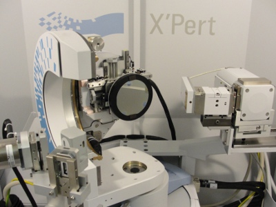
The Euler cradle of the diffractometer can scan over the whole of a 100 mm wafer, with precise control of tilt (χ) and rotation (φ).
The SiGe group is equipped with a Malvern Panalytical X'Pert PRO MRD high-resolution x-ray diffractometer, for the structural characterization of thin films.
The beam from the Cu x-ray tube passes through a hybrid 2-bounce asymmetric Ge(220) monochromator, which includes a mirror, such that an intense CuKα1 beam (λ=0.154 nm) is produced. An automatic beam attenuator can be used to extend the dynamic range of the system and protect the detector. The sample stage is able to map over 100 mm wafers, although there is space to mount 150 mm and 200 mm wafers (while a magnetic sample holder is used to mount smaller pieces). The diffracted beam can be passed through a 3-bounce symmetric analyzer crystal for high-resolution ω-2θ scans and reciprocal space maps.
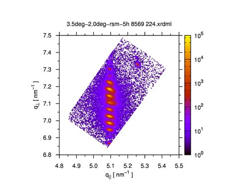
The system is used for symmetric and asymmetric reciprocal space mapping of semiconductor heterostructures, in particular the SiGe grown by LEPECVD. However, the system can also be used for analysis of polycrystalline materials, while very thin layers can be analyzed by in-plane diffraction, and other combinations of primary beam optics can be mounted.
Data are produced in the XRDML format.

A reciprocal space map, taken about the (224) reflection, of a SiGe heterostructure.
Copyright © 2010 L-NESS Como
