News - go back
| 3 Jun | 2021 | A singlet triplet hole spin qubit in planar Ge The IST Austria, in collaboration with the SiGe group and researchers from Barcelona and Konstanz, demonstrates a hole spin qubit in a double quantum dot device. With two spin-1/2 particles, the singlet |S⟩ = (|↑↓⟩-|↓↑⟩)/√2 and the unpolarised triplet |T0⟩ = (|↑↓⟩+|↓↑⟩)/√2 form the two computational-basis qubit states |0⟩ and |1⟩. In a weak magnetic field, electrically-tunable energy splitting between the ↑ and ↓ spin states in the two quantum dots allows the total spin state of the double quantum dot to be manipulated with nanosecond radiofrequency pulses. These short pulses means the qubit operations are very fast, while the long lifetime (150 μs) means that there would be time to perform complicated quantum computations. The state of the qubit can then be read electrically since the |S⟩ state allows current to tunnel through, while current is blocked by the |T0⟩ state. The use of an especially weak magnetic field - other work uses fields which are at least ten times stronger - would allow integration of these qubits with superconductors. The research is published in Nature Materials. DOI: 10.1038/s41563-021-01022-2. 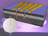
|
| 4 May | 2019 | First demonstration of antimatter wave interferometry It is the first version made with antimatter of the single particle interference experiment proposed by A. Einstein in 1927 and R. Feynman, for one of his famous lectures, and realized in 1976 by Merli, Missiroli and Pozzi, and in 1989 by A. Tonomura et al. This work has appeared on Science Advances and was realized by a collaboration that includes the Positron Laboratory of the Politecnico di Milano L-NESS in Como, where the experiment was performed. The others participating institutions are INFN (Milan unit), Università degli Studi di Milano, Università di Napoli Federico II and AEC & LHEP of the University of Bern. This is the first step of the QUPLAS (QUantum interferometry and gravity with Positrons and LASers) program. Link: https://advances.sciencemag.org/content/5/5/eaav7610 DOI: 10.1126/sciadv.aav7610 |
| 2 March | 2015 | The Positron Group has published (PNAS magazine) an advanced study on amorphous indium-gallium-zinc-oxide (IGZO) semiconductors in collaboration with the Group of Tobin Marks and Antonio Facchetti of the Northwestern University. In this work is demonstrated that the new coating technique, spray-combustion synthesis (SCS), produces IGZO films at low temperatures and in shorter times compared to the conventional sputtering technique. The properties of the IGZO films made by SCS, such as thickness, densification, nanoporosity, electron mobility, trap densities and bias stress stability, are at the same level of the sputtered films. It also determines the conditions of density and porosity that allow films with a good performance. Thin film transistors (TFT) IGZO has 50× higher electron mobility than amorphous silicon, which has often been used in displays (for smartphones, tablets, PCs, TVs, etc.). As a result, IGZO-TFT can improve the speed, resolution and size of flat-panel displays. It is thus considered to be one of the most promising TFT for use in organic light-emitting diode (OLED) displays. |
| 28 July | 2014 | The AEgIS collaboration at CERN has demonstrated a method to measure a very small deflection of an antimatter beam (smaller than the thickness of a human hair). The method has been tested by measuring the deviation of an antiproton beam (with the participation of a the Positron annihilation spectroscopy group). The research is published in Nature Communications. |
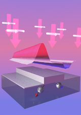
| 23 June | 2014 | The generation of two
complementary spin-up and spin-down electron
populations can be obtained by illuminating a semiconductor through a
patterned metal mask as shown in the Nature Materials
paper by an L-NESS-Physics Department and CNR team
|
| 12 May | 2014 | The fabrication of germanium-based modulators, detectors and waveguides on a silicon wafer offers an attractive platform for on-chip interconnects: the Silicon Photonics group of the University Paris Sud, in collaboration with the SiGe group, publishes in Nature Photonics.
La Provincia: Como, supermicrochip: Il Politecnico batte Stanford (in Italian) |
| 13 May | 2013 | The SiGe group is featured on TG Leonardo, reporting on the work recently published in Nature Photonics. |
| 2 May | 2013 | Nanobiotechnology experiments of controlled transport of nano-beads and release in cellular entities have been performed by Riccardo Bertacco and Daniela Petti of the NaBiS group on Geo Scienza on the italian TV channel RAI3. |
| 15 Apr | 2013 | Germanium is the laser material of the future
Researchers at the Politecnico together with the ETH Zurich and the Paul Scherrer Institute (Switzerland) have demonstrated how germanium can be transformed into a laser material. By making micro-bridges of germanium in which the reduction of the cross-section of the bridge at a constriction concentrates the pre-existing thermal stress left behind by the growth process, the bandgap is modified in a way which turns germanium into an efficient light emitter. The research is published in Nature Photonics |
| 10 Sep | 2012 | Built-in germanium lasers could make computer chips faster - research on material produced by the SiGe epitaxy group published in Physical Review Letters in collaboration with the PSI and ETH Zürich in Switzerland, highlights the conditions under which a germanium laser could be realized. |
| 03 Aug | 2012 | Graphene logic gates realized by the Nanoscale Device Group have been featured in NanotechWeb and PhysicsWorld |
| 24 Jul | 2012 | The Positron Group has published an advanced study on Hybrid Solar Cells in collaboration with the IIT (Italian Institute of Technology).
Hybrid solar cells are a combination of organic and inorganic materials. This new generation of thin-film is based on a very favourable price/performance ratio and the possibility to manufacture flexible and large-area modules. Positron Annihilation Spectroscopy using a variable-energy positron beam has been employed for the first time in this field in order to obtain depth-resolved data to study the infiltration of a conductive polymer (P3HT) into a mesoporous skeleton of titania. It has been possible to understand the reason of the improvement the device performance by engineering the hybrid interface using an inexpensive and transparent interlayer (4-mercaptopyridine). |
| 19 June | 2012 | The SuperFOx conference, organized by the Spintronics group, has been held in Como, 19-22th June 2012. |
| 8 Jun | 2012 | High-speed germanium quantum well modulator - Using high germanium content compounds is a promising approach to obtain efficient, high-speed modulation.
 |
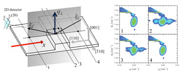
| 4 May | 2012 | X-ray diffraction maps uniaxial strain in a single nanostructure, work performed at ESRF beamline ID13 as a collaboration between the Nanoscale Device and SiGe epitaxy groups
 |
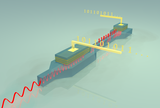
| 2 May | 2012 | The Spintronic group reported in Advanced Materials the first demonstration of Ge-based spin-photodiodes for integrated electrical detection of the polarization of light.
 |
| 16 Mar | 2012 | The SiGe epitaxy group makes the cover of Science for its work on Scaling Hetero-Epitaxy from Layers to Three-Dimensional Crystals in collaboration with the ETH Zürich, the Università di Milano-Bicocca and the Centre Suisse d'Electronique et de Microtecnique at Neuchâtel
Communicato stampa: Materiali perfetti? Ecco come ottenerli 
The cover of the 16th March issue of Science, featuring Ge crystals grown by LEPECVD on Si pillars. The growth was carried out at the L-NESS by Claudiu Falub, visiting from the ETH Zürich, and this scanning-electron microscopy image was taken by Claudiu at the ETHZ FIRST laboratory. |
| 23 Dec | 2011 | A graphene voltage amplifier realized by the Nanoscale Device Group has been featured in NanotechWeb |
| 3 Nov | 2011 | Dal Nobel al mercato: il grafene parla italiano (in Italian) - collaboration between the Nanoscale Device Group and Directa Plus |
| 14 Apr | 2011 | The Positron Annihilation Spectroscopy group featured in Così faremo volare davvero la nave di Star Trek da Como (in Italian) - video |
| 9 Nov | 2010 | Nanoribbons make good memories |
| 1 Sep | 2010 | The GREEN Silicon FET-Proactive EU Project begins, with the SiGe epitaxy group playing a fundamental role |
| 31 Aug | 2010 | L'iPhone e la Wii parlano anche comasco (in Italian) |
| 6 Apr | 2010 | Spintronics wins Cariplo grant for SpinBioMed |
| 18 Jan | 2010 | New L-NESS website goes online |
| 1 Nov | 2009 | The 8th ESPS-NIS will be held in Como, 14-18th June 2010 |
| 7 Apr | 2008 | Il Sole 24 ORE visit the L-NESS |
Copyright © 2010 L-NESS Como