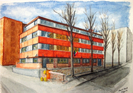
L-NESS - see News
The L-NESS - Laboratory for Nanostructure Epitaxy and Spintronics on Silicon - occupies a unique position in the Italian research landscape because of the extraordinary concentration of research infrastructure:
- advanced deposition equipment for semiconductor and oxide hetero-epitaxy:
- SiGe low-energy plasma-enhanced chemical vapor deposition (LEPECVD)
- III-V MBE with in-situ RHEED
- deposition of epi-oxides and metals (PLD/MBE cluster tool with in-situ XPS/UPS, IPES, RHEED, LEED; magnetron sputtering cluster tool) for spintronics and nanomedicine
- advanced e-beam lithography fabrication facility (nanoscale device group).
- advanced characterization equipment for thin films, with a special emphasis on the characterization of advanced heterostructures and defects in materials.
- advanced atomistic modelling know-how (ab initio and semi-empirical).
Due in part to the origins of the centre, the L-NESS workforce is very international, and English is commonly used as the working language. Active research links are maintained with research labs located
- in Europe
- ETH (Zürich)
- Max Planck Institute for Solid State Research (Stuttgart)
- Paul Scherrer Institut (Villigen)
- Philipps-Universität Marburg
- Université Paris-Sud
- Minatec (Grenoble)
- Université Paul Cézanne (Marseille)
- IMEC (Leuven)
- Helsinki University of Technology
- CIC nanoGUNE (San Sebastián)
- DTU Nanotech (Copenhagen)
- COBRA Research Institute (Eindhoven)
- and elsewhere in the world
The multidisciplinary approach of the L-NESS is reflected in intense collaborations among researchers active in the growth of materials, their characterization, and their atomistic modeling. Finally, a strong emphasis is placed on developing strategic partnerships with the global high-tech industry.
Copyright © 2010 L-NESS Como
