Nanoscale Device Group
Research
- Graphene nanoelectronics
- Semiconductor nanofluidic devices for nanomedicine
- Nanoelectronics in semiconductor heterostructures
- Nanopatterning of semiconductor substrates
Graphene nanoelectronics
Graphene, a recently isolated single sheet of graphite, is currently being investigated as a viable alternative to Si for the channel of field-effect transistors (FETs) at the sub-10 nm scale, at which the ultimate limits of Si technology would probably be reached. The high mobility of carriers in graphene could allow fabrication of FETs with a very low channel resistance, resulting in a high operational speed. The remarkable electronic properties of graphene and its compatibility with Si lithographic techniques promise to simplify the transition to carbon-based electronics. Large-scale fabrication of graphene is currently being attempted by epitaxial growth, transfer printing, deposition from a solution, or anodic bonding.
Our group is interested in the development of graphene nanoelectronic devices. We developed the first logic gates and the first integrated circuit (complementary inverter) on graphene.
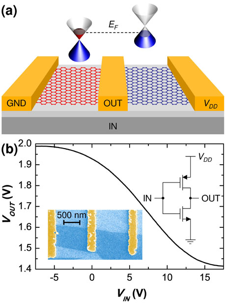
A schematic of the fabricated integrated complementary graphene inverter is shown in Fig. 1. We isolated graphene on an insulating substrate by peeling graphene flakes from a piece of graphite with an adhesive tape. The same method was used to isolate graphene for the first time. We fabricated two transistors on the same graphene flake by electron beam lithography. The key to obtaining a functional integrated circuit was to change the type of one of the transistors from p to n by Joule heating. An ideal graphene transistor is n-type, meaning that electrons pass current, when a positive voltage is applied to the gate but p-type when a negative voltage is applied. Contamination from oxygen and water vapour in the air, however, causes the switchover "Dirac" point to shift from zero to a positive voltage, making the transistor p-type. We passed a large current through one transistor and the heating effect of the current removed the contaminants, shifting its Dirac point back and therefore restoring n-type behaviour. In this way we obtained two transistors of opposite type integrated on the same graphene flake. This pair of transistors forms a digital logic inverter, a basic building block of CMOS.

Fig. 1. Integrated complementary graphene inverter. (a) A schematic of the fabricated inverter. Three electrodes patterned on the same flake of monolayer graphene define two FETs. The part of the flake between the two leftmost electrodes (depicted in red) is electrically annealed to obtain an n-type FET. The other part of the flake (depicted in blue) is a p-type FET. (b) The measured DC voltage transfer characteristics of the fabricated complementary graphene inverter. Insets: SEM image of the fabricated inverter and the circuit layout.
Research on graphene has been done in collaboration (μRaman) with the Micro and nanostructured materials lab, Politecnico di Milano, Italy.
Semiconductor nanofluidic devices for nanomedicine
Biochemical reactions usually involve a large number of protein and nucleic acid molecules interacting at the nanoscale. Exploring the microscopic basis of such reactions is often obscured because averaged responses from an enormous number of individual molecules are measured in the experiment. Ability to separate, isolate, and investigate a small number of molecules in a nanoscale-confined environment is a long-sought goal of molecular diagnostics.
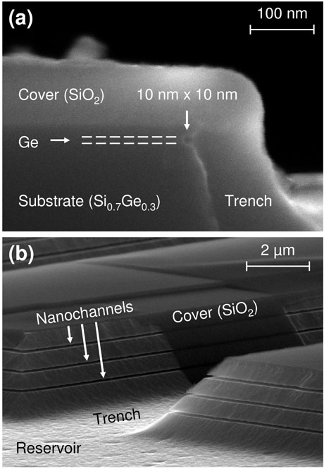
The affordability of a molecular diagnostic platform is commonly at odds with the nanoscale requirements of single-biomolecular studies. To overcome this constraint, we developed an alternative technology capable of producing nanofluidic channels without expensive (in terms of cost per chip) top-down nanolithography. The vertical arrays of nanochannels are fabricated from a heterostructure comprised of a substrate and several thin sacrificial layers. The heterostructure is etched deep enough to expose the lateral surface of the required number of sacrificial layers which are then selectively wet-etched laterally to form the nanochannels. The fabricated nanochannels are shown in Fig. 2.

Fig. 2. Nanofluidic channels fabricated in two different types of SiGe heterostructure. (a) A single nanochannel structure obtained by a selective side etching of a Ge sacrificial layer on a Si0.3Ge0.7 virtual substrate. The nanochannel runs perpendicular to the image and has a cross-section of 10 nm × 10 nm. (b) A structure with three nanochannels obtained by etching Si0.6Ge0.4 sacrificial layers on a Si substrate. The nanochannels have a cross-section of 130 nm × 100 nm.
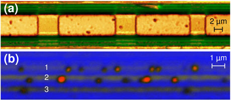
The present fabrication process is compatible with standard semiconductor technology enabling simple integration with conventional electronic and fluidic devices for fast on-chip processing. The suitability of the fabricated nanochannels for nanofluidic applications is demonstrated by observing the flow of a fluorescent dye solution through the nanochannels with the help of a confocal laser scanning microscope (Fig. 3). The potential utility of the nanochannels in biologically relevant applications - e.g., size-based separation of biomolecules - is demonstrated by imaging aggregates of amyloid beta, the amyloidogenic peptide implicated in Alzheimer's disease. The size of the amyloid beta aggregate that can enter a nanochannel is found to be dependent on the channel cross-section (Fig. 3).

Fig. 3. Overlay (reflection and fluorescence) confocal images of the nanochannels. (a) A three nanochannel Si/Si0.6Ge0.4 structure in which the nanochannels are filled with fluorescent dye (green signal). (b) Labelled amyloid beta aggregates in the nanochannels. The smaller nanochannel (marked by 1) has a cross-section of 260 nm × 300 nm. The larger nanochannel (marked by 2) has a cross section of 310 nm × 300. The mostly empty nanochannel (marked by 3) has a cross section of 350 nm × 300 nm. Large aggregates are found only in the nanochannel 2, while small aggregates are visible both in nanochannels 1 and 2.
Research on nanofluidics has been done in collaboration with the Nanoscale Diagnostics Group, Max Planck Institute for Solid State Research, Germany and Department of Experimental Medicine, University of Milan - Bicocca, Italy.
Nanoelectronics in semiconductor heterostructures
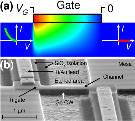
The research on low-dimensional systems has mainly been focused on field effect transistors, yet many conventional applications cannot be realized without diodes. For this reason one of the nanostructures we developed was a gate-controlled rectifier. The use of gate-induced junctions opens a route to reconfigurable electronic devices and provides valuable insight into the understanding of low-dimensional nanostructures. The fabricated gate-controlled diode is shown in Fig. 4. The diode was fabricated by patterning a SiGe modulation doped heterostructure grown by LEPECVD. A forward-to-reverse current ratio of more than 104 was obtained.

Fig. 4. Gate-controlled rectifier. (a) Potential distribution along the gate and potential induced by the gate inside the semiconductor. (b) SEM image of the nanofabricated diode. The Ge has been etched faster than the surrounding Si0.3Ge0.7, so the location of the Ge quantum well (QW) can be identified by a dark narrow slit 83 nm below the top surface.
Nanopatterning of semiconductor substrates
The templates for pre-patterning of Si substrates for subsequent quantum dot growth by LEPECVD were developed and successfully tested both in PMMA and by a lift-off process. These patterns consist of dots or perpendicular lines which will be transferred to the substrate as pits or trenches after reactive ion etching. The patterns will be transferred to the substrates together with the alignment marks for the second-level patterning of metal electrodes. It is planned to address individual quantum dots and realize single-electron and resonant tunneling transistors.
Copyright © 2010 L-NESS Como
