Nanoscale Device Group
Facilities
- Electron beam lithography
- E-beam evaporators
- Probe stations
- Optical lithography
- Atomic force microscopy
- He cryostat
- Clean room
Electron beam lithography
The ever-growing demand for increasing the integration scale of digital electronics has prompted a search for novel devices and fabrication techniques at the nanometer scale. State-of-the-art deep ultra violet (DUV) and extreme ultra violet (EUV) lithographies are expected to deliver transistors with the gate length as small as 10 nm at the 5-7 nm nodes in 2020. Electron beam lithography (EBL) is an indispensable technique for making the nanoelectronic devices on a similar scale in research setting (Fig. 1).

Fig. 1. The high-resolution structures patterned by our EBL systems on standard SiO2/Si substrates. (top-left) 7-nm wide lines patterned by our Raith eLINE system in HSQ resist. (top-right) 11-nm wide metallic line patterned by our old EBL system in 200 nm thick PMMA resist. The line consists of 3 nm of Cr and 10 nm of Au. The scale bar is the same in both images. (bottom) Our Raith eLINE system is capable of patterning high-resolution structures (as shown in the top-left image) on 100-mm wafers because it has a high-precision laser interferometer stage and laser height sensing (i.e., auto focus).
In this technique, a highly focused electron beam is scanned over a surface covered by a resist sensitive to electron radiation (e.g., polymethyl-methacrylate - PMMA). Exposed areas become more (positive resist) or less (negative resist) soluble in organic solvents (e.g., methyl isobutyl ketone - MIBK), which are used to develop the exposed pattern. The pattern is transferred to the substrate by etching (e.g., reactive ion etching) or lift-off (e.g., metallization).
While the resolution of DUV lithography is mostly limited by the wavelength of the ArF excimer laser, diffraction is not the limiting factor in EBL due to a very small electron wavelength (less than 0.01 nm at 20 keV). The resolution of EBL is mostly limited by imperfections in the electron optics (aberrations limit the minimum electron beam spot size to ~ 1 nm) and electron scattering in resist and backscattering from the substrate. These effects limit the smallest feature size to ~ 10 nm after lift-off.
EBL is not suitable for a large scale production because electron beam exposure is a serial process (i.e., it is much slower than EUV or DUV lithography). On the other hand, EBL is a fabrication tool of choice in nanoelectronics and low-dimensional physics. It allows researchers to fabricate and investigate very small devices which might be used in the future. The main advantage of EBL in research setting is its direct write capability, i.e., no need for making a mask as required by an EUV or DUV lithography. EBL is used industrially in mask making for EUV or DUV lithography.
The work on EBL in Como started in May 2005 with the installation of a scanning electron microscope (SEM) with a lithography attachment. The group is currently equipped with two EBL systems:
- Raith eLINE (shown in Fig. 2) is a fully integrated EBL system. The main features are: Schottky field-emission gun, acceleration voltage up to 30 kV, high-speed pattern generator (20 MHz), laser interferometer stage with a stitching error < 20 nm and 100 x 100 mm horizontal and 30 mm vertical travel range under full interferometric control, alignment error < 20 nm, automated laser height sensing (i.e., auto focus with a working distance error < 5 µm), traxx module for stitching error free continuous writing mode for elongated paths (fixed-beam moving stage mode - FBMS), 3D module, and manual load-lock.
- Philips XL30 SFEG SEM with a Raith Elphy Quantum lithography attachment (6 MHz pattern generator) and a Scanservice beam blanker. This is our original EBL system (shown in Fig. 3) which is mainly used as a backup now.
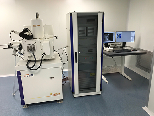
Fig. 2. Our Raith eLINE system. The EBL resolution limit is ~ 7 nm, corresponding to the width of the lines patterned in a thin HSQ resist at 30 kV.
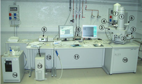
Fig. 3. Our old EBL system. Parts: 1. Column 2. Specimen chamber 3. Secondary electron detector 4. Scanservice final aperture with integrated beam blanker 5. CCD camera 6. High tension valve 7. Liquid N2 tank (for X-ray detector) 8. Keithley pico-ammeter (to measure beam current) 9. Beam blanker power supply 10. Vacuum pumps and high tension circuitry 11. Electronics (printed circuits boards) 12. Power supply 13. Lithography PC (Raith Elphy Quantum) 14. SEM PC with integrated X-ray analyzer.
E-beam evaporators
The group is equipped with two e-beam evaporators. One evaporator is outside of the clean room and used only for large wafers. Our group mostly use the other evaporator which is located in the clean room and used for chips.
Probe stations
The electrical characterizations of our graphene electronic devices are performed in two FormFactor probe stations, Summit 11000 (shown in Fig. 4) and EP6, both by dc and real-time high-frequency measurements. The dc measurements are based on Keithley SMUs (five 2611A and one 2636B), while Keysight 4 GHz and 16 GHz scopes are used for real-time measurements.
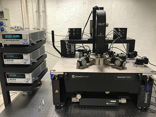
Fig. 4. Our FormFactor Summit 11000 (200 mm) probe station.
Optical lithography
The state-of-the-art ArF DUV lithography is out of reach of most research groups and is commercially used by big semiconductor companies to fabricate integrated circuits. The research groups usually use much less expensive optical lithography in which longer wavelengths (typically, i-line at 365 nm) are used to expose photoresists. This increases the smallest feature size to ~ 500 nm. Our group does not use optical lithography so much because the minimum feature size in our optical process is ~ 1 µm (compare it to the smallest feature size of ~ 6 nm of our eLINE EBL system) which is unsuitable for the nanofabrication of short-channel graphene field-effect transistors. Photoresists are also more detrimental to electrical properties of graphene than PMMA.
Our group is equipped with a Karl Suss MA56 mask aligner (shown in Fig. 5) capable of contact and proximity printing on 4” wafers and 5” masks by i-line, 20 mWcm-2). The aligner is mainly used to pattern SiGe heterostructures (e.g., into Hall bars on which nanostructures are overlaid by EBL).
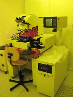
Fig. 5. Our Karl Suss MA56 mask aligner.
Atomic force microscopy
The group is equipped with a Veeco Innova atomic force microscope (shown in Fig. 6). The microscope is used to scan graphene devices and quantum dots grown on pre-patterned Si substrates.
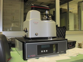
Fig. 6. Our Veeco Innova atomic force microscope.
He cryostat
The group is equipped with a Cryogenic cryogen free (i.e., a closed cycle liquid helium-4) cryostat (shown in Fig. 7) with a superconducting magnet (fields up to 7.5 T) and an integrated variable temperature insert. The lowest temperature which can be reached by this cryostat is ~ 1.4 K. The cryostat is connected to a transport measurement system comprised of digital source meters, multi meters, preamplifiers, function generators, an oscilloscope, and an acquisition board. This system is used for the characterization of fundamental investigations of nanodevices (devices for realistic applications are investigated in the probe stations in air ambient).
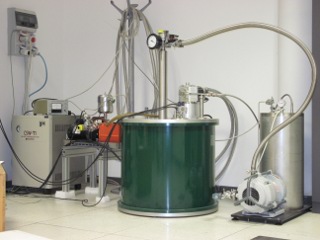
Fig. 7. Our Cryogenic liquid helium-4 cryostat.
Clean rooms
We have two ISO 6 clean rooms in which all device processing is done. The first clean room is equipped with a mask aligner, an e-beam evaporator, ovens, spin-coaters, wet benches, ultrasonic baths, a plasma asher, and an optical microscope. The second clean room (shown in Fig. 8) is fully dedicated to our Raith eLINE system.
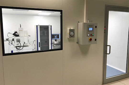
Fig. 8. One of our clean rooms which is housing our Raith eLINE.
Copyright © 2010 L-NESS Como